Method and system for patterning a substrate

a substrate and patterning technology, applied in the field of device manufacturing, can solve the problems of difficult to achieve the desired resolution of the pattern, time-consuming and costly process, and difficult manipulation of soft x-rays or extreme ultraviolet radiation using mirrors and/or optical lenses,

Inactive Publication Date: 2011-12-08
VARIAN SEMICON EQUIP ASSOC INC
View PDF4 Cites 26 Cited by
  • Summary
  • Abstract
  • Description
  • Claims
  • Application Information

AI Technical Summary

Problems solved by technology

However, limitations in forming a mask with a desired resolution and having compatibility with the properties (e.g. wavelength) of the radiation used in the patterning process have led to difficulties in achieving patterns with the desired resolution.
Although the technique is capable of forming the patterns with fine resolution, the process is very time consuming and costly.
However, soft x-rays or extreme UV radiation are difficult to manipulate using mirrors and/or optical lenses.
In addition, using soft x-rays or extreme UV radiation to pattern a

Method used


Image

  • Method and system for patterning a substrate
  • Method and system for patterning a substrate
  • Method and system for patterning a substrate

Examples


Embodiment Construction

[0035]The present disclosure will now be described more fully hereinafter with reference to the accompanying drawings, in which preferred embodiments are shown. This disclosure, however, may be embodied in many different forms and should not be construed as limited to the embodiments set forth herein. Rather, these embodiments are provided so that this disclosure will be thorough and complete, and will convey the scope of the invention to those skilled in the art. In the drawings, like numbers refer to like elements throughout.

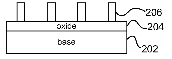
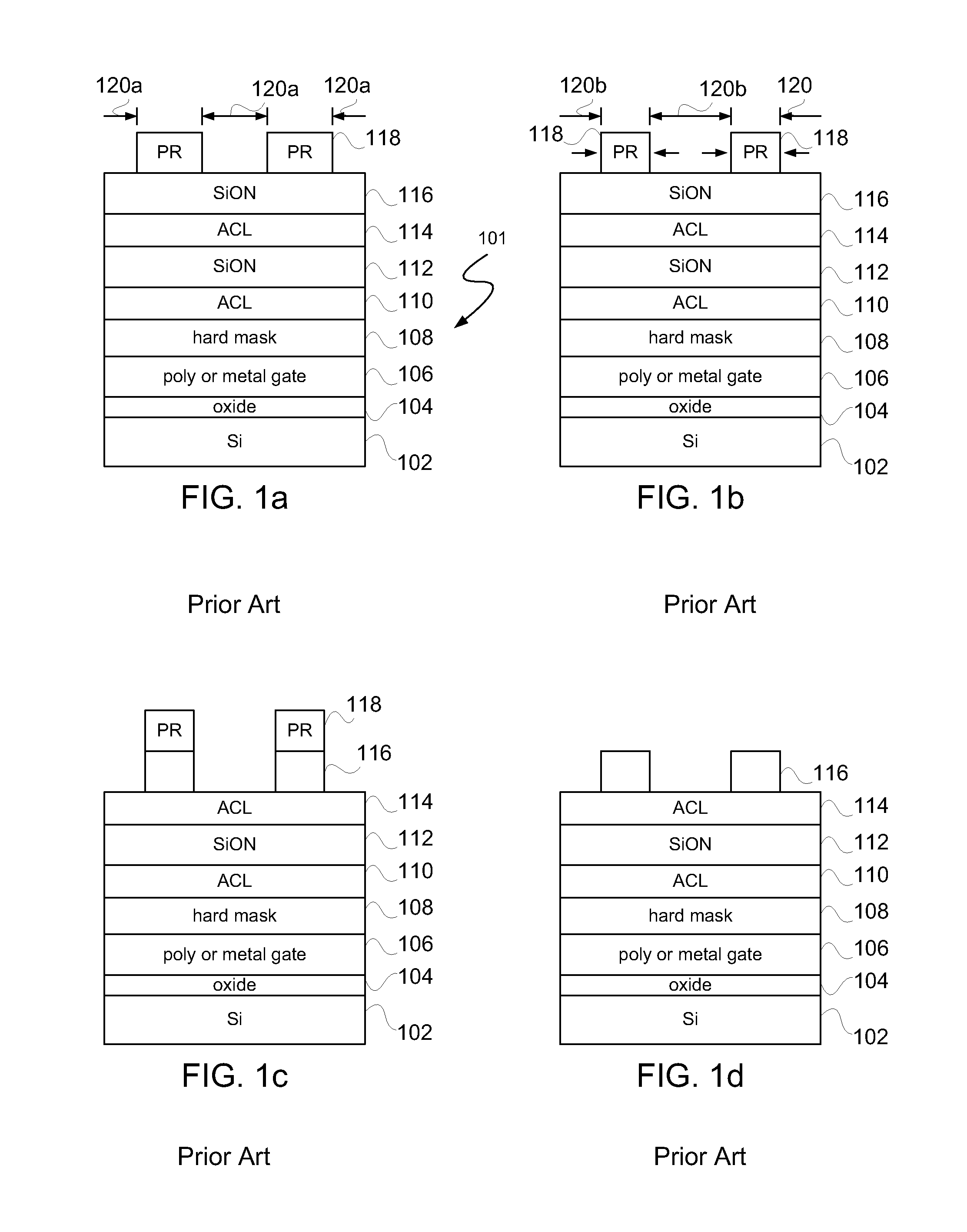
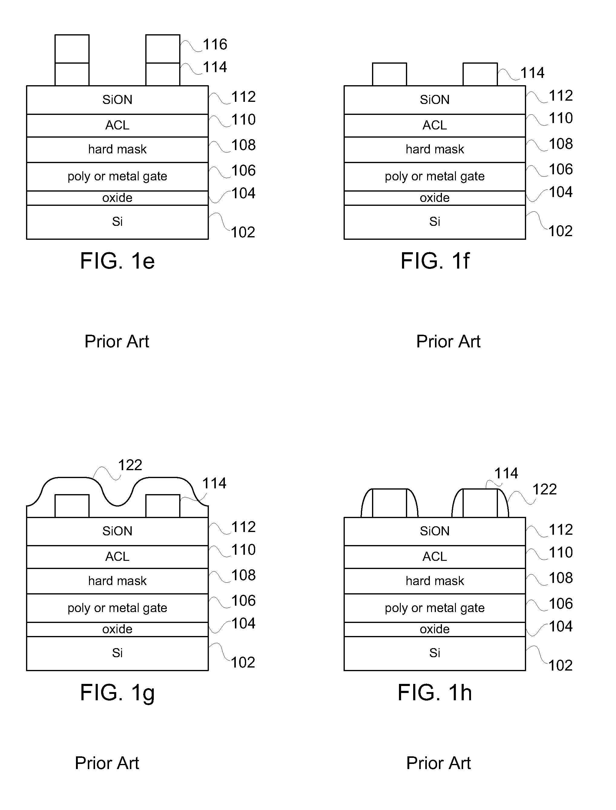
[0036]To solve the deficiencies associated with the methods noted above, novel and inventive techniques for patterning a substrate are introduced. For purposes of clarity and simplicity, the present disclosure focuses on techniques to pattern a substrate for forming transistors.

[0037]In particular, the present disclosure focuses on techniques involving SADPL processes for forming gates of transistors. However, those of ordinary skill in the art will recognize ...


PUM


Abstract

A method of patterning a substrate comprises providing an array of resist features defined by a first pitch and a first gap width between adjacent resist features. Particles are introduced into the array of resist features, wherein the array of resist features becomes hardened. The introduction of particles may cause a reduction in critical dimension of the resist features. Sidewalls are provided on side portions of hardened resist features. Subsequent to the formation of the sidewalls, the hardened resist features are removed, leaving an array of isolated sidewalls disposed on the substrate. The sidewall array provides a mask for double patterning of features in the substrate layers disposed below the sidewalls, wherein an array of features formed in the substrate has a second pitch equal to half that of the first pitch.

Description

[0001]This application claims priority to U.S. provisional patent application Ser. No. 61 / 235,383, filed Aug. 20, 2009, and incorporated by reference herein in its entirety.BACKGROUND OF THE INVENTION[0002]1. Field of the Invention[0003]Embodiments of the invention relate to the field of device manufacturing. More particularly, the present invention relates to a method, system and structure for patterning a substrate for manufacturing a device.[0004]2. Discussion of Related Art[0005]In forming electronic devices, patterning processes are widely used. As known in the art, there exist various types of patterning processes. One example of the process is a photolithographic patterning process by which a pattern of desired resolution is transferred optically from an optical mask to a photoresist layer deposited onto the substrate and, ultimately, to the substrate. In one example, patterning has been used on a substrate to form the gate of a field effect transistor.[0006]With continuing m...

Claims


Application Information

Patent Timeline
IPC IPC(8): H01L21/311G21K5/00H01L21/263
CPCG03F7/40G03F7/405H01L21/32139H01L21/0337H01L21/0273
Inventor MARTIN, PATRICK M.CARLSON, STEVENOH, CHOONG-YOUNGPARK, JUNG-WOOK
Owner VARIAN SEMICON EQUIP ASSOC INC
Why Eureka
Try Eureka