Semiconductor device and fabrication method therefor

a technology of semiconductor devices and fabrication methods, applied in semiconductor devices, electrical devices, transistors, etc., can solve the problems of high-doping silicon layer resistance, leakage current, and difficulty in operating as a transistor of semiconductor devices, and achieve the effect of increasing the resistance of high-doping silicon layers

Active Publication Date: 2011-12-15
UNISANTIS ELECTRONICS SINGAPORE PTE LTD
View PDF5 Cites 120 Cited by
  • Summary
  • Abstract
  • Description
  • Claims
  • Application Information

AI Technical Summary

Benefits of technology

[0012]Usually, in a MOS transistor, the metal-silicon compound layer formed on the highly doped silicon layer acting as a gate electrode, a source, and a drain is formed in the same processing step. Also in an SGT, the metal-silicon compound layer formed on the highly doped silicon layer acting as a gate electrode, a source, and a drain is formed in the same processing step as well as the MOS transistor. Therefore, in the SGT, when forming a thick metal-silicon compound layer in either of the highly doped silicon layers acting as a gate electrode, source, and drain, a metal-s...

Problems solved by technology

Accordingly, it becomes difficult for the SGT to operate as a transistor.
Therefore, it becomes d...

Method used


Image

  • Semiconductor device and fabrication method therefor
  • Semiconductor device and fabrication method therefor
  • Semiconductor device and fabrication method therefor

Examples


first embodiment

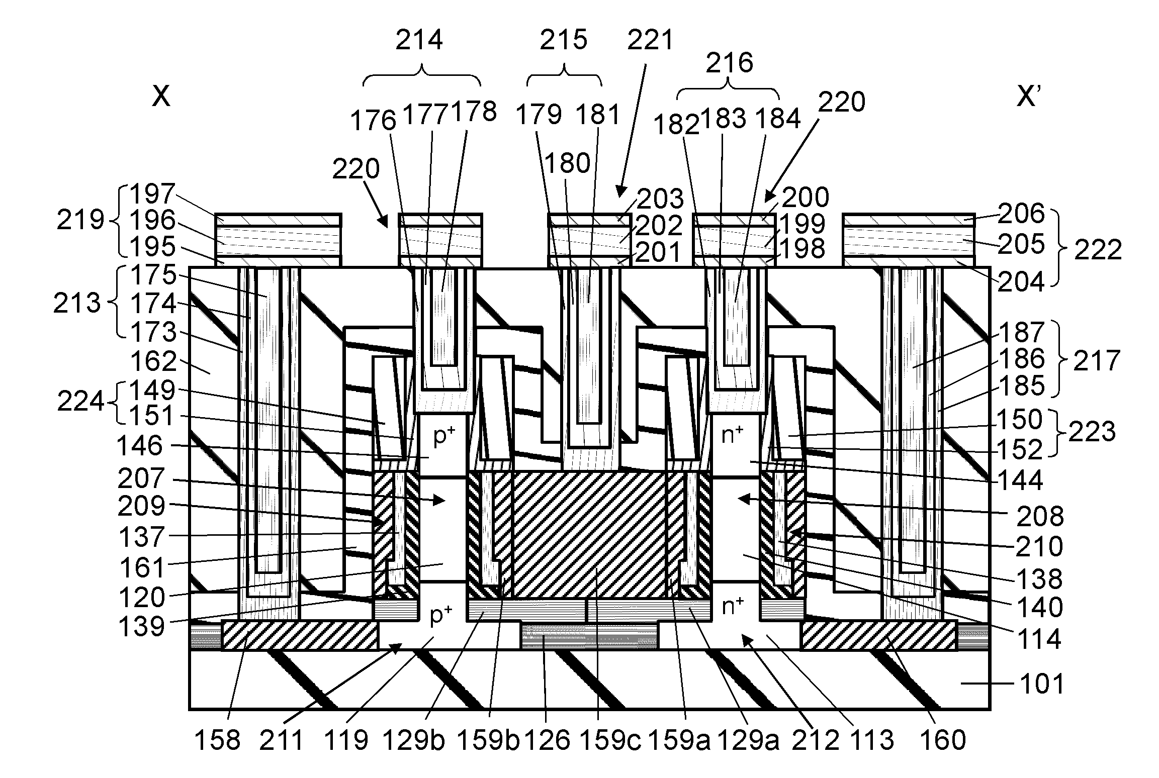
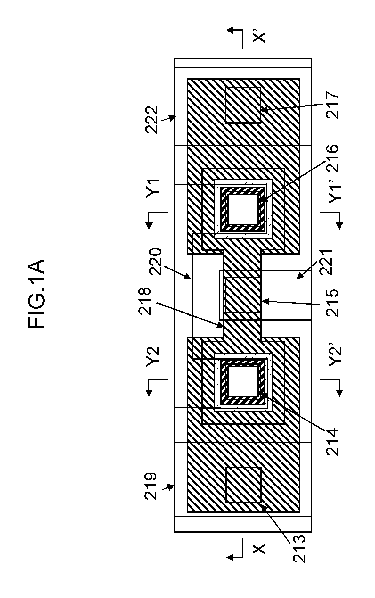
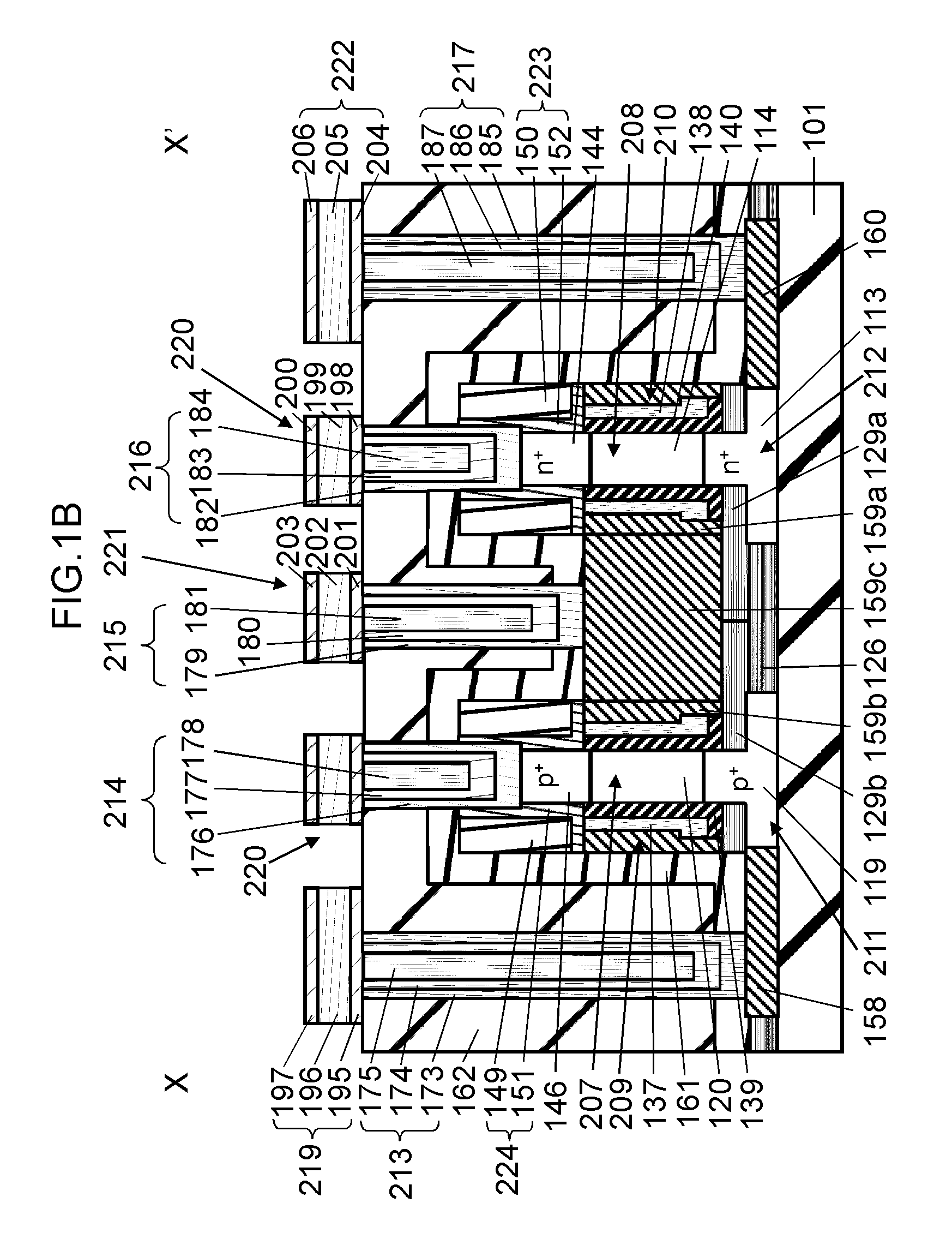
[0234]FIG. 1A is a top view showing an inverter including Negative Channel Metal-Oxide-Semiconductor (NMOS)-SGT and Positive Channel Metal-Oxide-Semiconductor (PMOS)-SGT according to a first embodiment of the present invention, and FIG. 1B is a cross-sectional diagram taken in the cutting line X-X′ of FIG. 1A. FIG. 2A is a cross-sectional diagram taken in the cutting line Y1-Y1′ of FIG. 1A. FIG. 2B is a cross-sectional diagram taken in the cutting line Y2-Y2′ of FIG. 1A. Although FIG. 1A is a top view, hatching is attached in part in order to distinguish an area.

[0235]With reference to FIG. 1A to FIG. 2B, the inverter including the NMOS-SGT and PMOS-SGT according to the first embodiment will be explained hereinafter.

[0236]First of all, the NMOS-SGT of the first embodiment will be explained. A first planar silicon layer 212 is formed on a silicon dioxide film 101, and a first columnar silicon layer 208 is formed on the first planar silicon layer 212.

[0237]A first n+ type silicon laye...


PUM


Abstract

The semiconductor device includes: a columnar silicon layer on the planar silicon layer; a first n+ type silicon layer formed in a bottom area of the columnar silicon layer; a second n+ type silicon layer formed in an upper region of the columnar silicon layer; a gate insulating film formed in a perimeter of a channel region between the first and second n+ type silicon layers; a gate electrode formed in a perimeter of the gate insulating film, and having a first metal-silicon compound layer; an insulating film formed between the gate electrode and the planar silicon layer, an insulating film sidewall formed in an upper sidewall of the columnar silicon layer; a second metal-silicon compound layer formed in the planar silicon layer; and an electric contact formed on the second n+ type silicon layer.

Description

RELATED APPLICATIONS[0001]This patent application claims the benefit of U.S. Patent Provisional Application 61 / 352,961, filed Jun. 9, 2010, and Japanese Patent Application 2010-132488, filed Jun. 9, 2010, the entire disclosures of which are incorporated herein.BACKGROUND OF THE INVENTION[0002]1. Field of the Invention[0003]This application relates to a semiconductor device and a fabrication method therefor.[0004]2. Description of the Related Art[0005]High integration of a semiconductor integrated circuit and an integrated circuit especially using an MOS transistor has been enhanced.[0006]Miniaturization has been developed to a nano region of a Metal-Oxide-Semiconductor (MOS) transistor used in an integrated circuit with high integration of the semiconductor integrated circuit. When the miniaturization of the MOS transistor progressed, control of leakage current is difficult. Furthermore, there was a problem that it cannot make an occupation area of a circuit easily small in order to...

Claims


Application Information

Patent Timeline
IPC IPC(8): H01L27/092H01L21/336H01L29/78
CPCH01L21/823885H01L21/84H01L29/66484H01L29/42392H01L29/78642H01L27/1203H01L27/105
Inventor MASUOKA, FUJIONAKAMURA, HIROKIARAI, SHINTAROKUDO, TOMOHIKOJIANG, YUCHUI, KING-JIENLI, YISUOLI, XIANGCHEN, ZHIXIANSHEN, NANSHENGBLIZNETSOV, VLADIMIRBUDDHARAJU, KAVITHA DEVISINGH, NAVAB
Owner UNISANTIS ELECTRONICS SINGAPORE PTE LTD
Why Eureka
Try Eureka