
Semiconductor package with heat dissipation devices

Active Publication Date: 2011-12-15
SK HYNIX INC
View PDF3 Cites 43 Cited by
  • Summary
  • Abstract
  • Description
  • Claims
  • Application Information

AI Technical Summary

Benefits of technology

[0008]An embodiment of the present invention is directed to a semiconductor package which can improve a heat dissipation characteristic.
[0009]Also, an embodiment of the present invention is directed to a semiconductor package which can achieve an improved operation characteristic.

Problems solved by technology

Hence, as power consumption per unit volume increases, heat generated during the operation of a memory chip raises the temperature of a package.
Such a temperature rise results in a decrease in the operation speed of a semiconductor package.
However, since a conventional semiconductor package has a structure in which a memory chip is smaller than a substrate it is mounted on, a problem is that it is not easy to dissipate heat from a portion of the substrate where the memory chip is not disposed.
In particular, since the portion of the substrate where the memory chip is not disposed is sealed by a substance with poor heat conductivity, such as an EMC (epoxy molding compound), so as to protect the package, the portion of the substrate is not likely to appropriately dissipate a large amount of heat generated during operation of the memory chip.
Consequently, in the conventional semiconductor package, since it is not easy to dissipate the heat generated during the operation of the memory chip, the temperature of the package rises and the operation characteristic of the package may deteriorate.

Method used


Image

  • Semiconductor package with heat dissipation devices
  • Semiconductor package with heat dissipation devices
  • Semiconductor package with heat dissipation devices

Examples


first embodiment

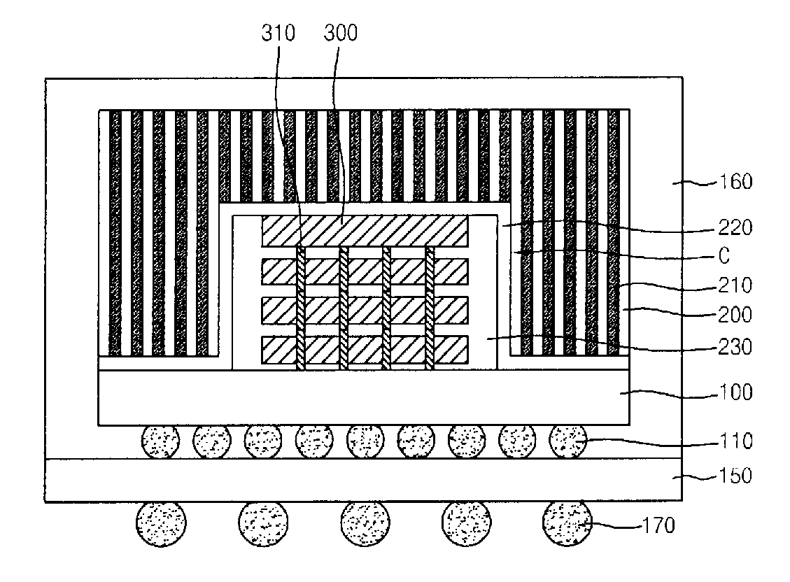
[0043]FIG. 1 is a cross-sectional view illustrating a semiconductor package in accordance with the present invention.

[0044]Referring to FIG. 1, a first semiconductor chip 100, on which second semiconductor chips 300 and a heat dissipation member 200 are disposed, is mounted to an upper surface of a substrate 150, which has the upper surface and a lower surface facing away from the upper surface, by the medium of connection members 110. The first semiconductor chip 100 may be a logic chip or a memory chip.

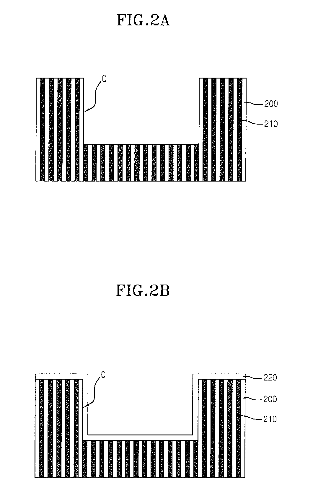
[0045]In detail, the first semiconductor chip 100 has a first surface and a second surface which faces away from the first surface. The heat dissipation member 200, which is formed of a ceramic material such as, for example, silicon or glass, is disposed over the first surface of the first semiconductor chip 100. The heat dissipation member 200 has a cavity C, and a plurality of metal pillars 210 are installed in the heat dissipation member 200 around the cavity C, that is, on both ...

second embodiment

[0065]Meanwhile, although it was described and illustrated in the above embodiment that the first semiconductor chip with the second semiconductor chips and the heat dissipation member disposed thereon is mounted to the substrate by the medium of the connection members, in the present invention, external connection terminals may be directly disposed on distribution lines which are formed on the second surface of a first semiconductor chip without using a substrate.

[0066]FIG. 3 is a cross-sectional view illustrating a semiconductor package in accordance with a second embodiment of the present invention.

[0067]Referring to FIG. 3, redistribution pads 120 are disposed on the second surface of a first semiconductor chip 100 on which second semiconductor chips 300 and a heat dissipation member 200 are disposed. Redistribution lines 130 are formed to be electrically connected with the redistribution pads 120, and an insulation layer 140 is formed on the second surface of the first semicond...

third embodiment

[0068]Although it was described and illustrated in the aforementioned embodiments that the heat dissipation member is formed such that the metal pillars are installed not only on both sides of the cavity but also over the cavity to dissipate heat from both sides and over the second semiconductor chips, it can be envisaged in the present invention that metal pillars are not additionally installed over the second semiconductor chips since heat can be relatively easily dissipated and are installed only on both sides of the second semiconductor chips since heat cannot be easily dissipated, so that the height of a semiconductor package can be decreased.

[0069]FIG. 4 is a cross-sectional view illustrating a semiconductor package in accordance with a third embodiment of the present invention.

[0070]Referring to FIG. 4, a first semiconductor chip 100, on which second semiconductor chips 300 and a heat dissipation member 200 are disposed, is mounted to an upper surface of a substrate 150, whic...


PUM


Abstract

A semiconductor package includes a first semiconductor chip having a first surface and a second surface which faces away from the first surface, a heat dissipation member, defined with a cavity, disposed on the first surface of the first semiconductor chip and having a plurality of metal pillars which contact the first semiconductor chip, and one or more second semiconductor chips stacked on the first surface of the first semiconductor chip in the cavity to be electrically connected with one another and with the first semiconductor chip.

Description

CROSS-REFERENCE TO RELATED APPLICATIONS[0001]The present application claims priority to Korean patent application number 10-2010-0054413 filed on Jun. 9, 2010, which is incorporated herein by reference in its entirety.BACKGROUND OF THE INVENTION[0002]The present invention relates to a semiconductor package, and more particularly, to a semiconductor package which can improve a heat dissipation characteristic and achieve an improved operation characteristic.[0003]These days, the electronic industry trends to manufacture products at reduced costs with high reliability in such a way as to accomplish light weight, miniaturization, high speed operation, multi-functionality, and high performance. A package assembly technology is important for achieving such purposes. The package assembly technology protects memory chips, having integrated circuits formed therein through a wafer fabrication process, and allows those chips to be easily mounted to a substrate so that operational reliability o...

Claims


Application Information

Patent Timeline
IPC IPC(8): H01L23/48
CPCH01L23/3128H01L23/3675H01L23/3736H01L23/42H01L23/49816H01L2924/09701H01L2224/16145H01L2225/06513H01L2225/06517H01L2225/06565H01L2225/06589H01L25/0657H01L2924/16251
Inventor SON, HO YOUNG
Owner SK HYNIX INC
Learn More