Plasma treatment at a p-i junction for increasing open circuit voltage of a photovoltaic device
a photovoltaic device and open circuit technology, applied in the field of plasma treatment process for forming a photovoltaic device, can solve problems such as heat generation of irradiated materials
- Summary
- Abstract
- Description
- Claims
- Application Information
AI Technical Summary
Benefits of technology
Problems solved by technology
Method used
Image

Examples
Embodiment Construction
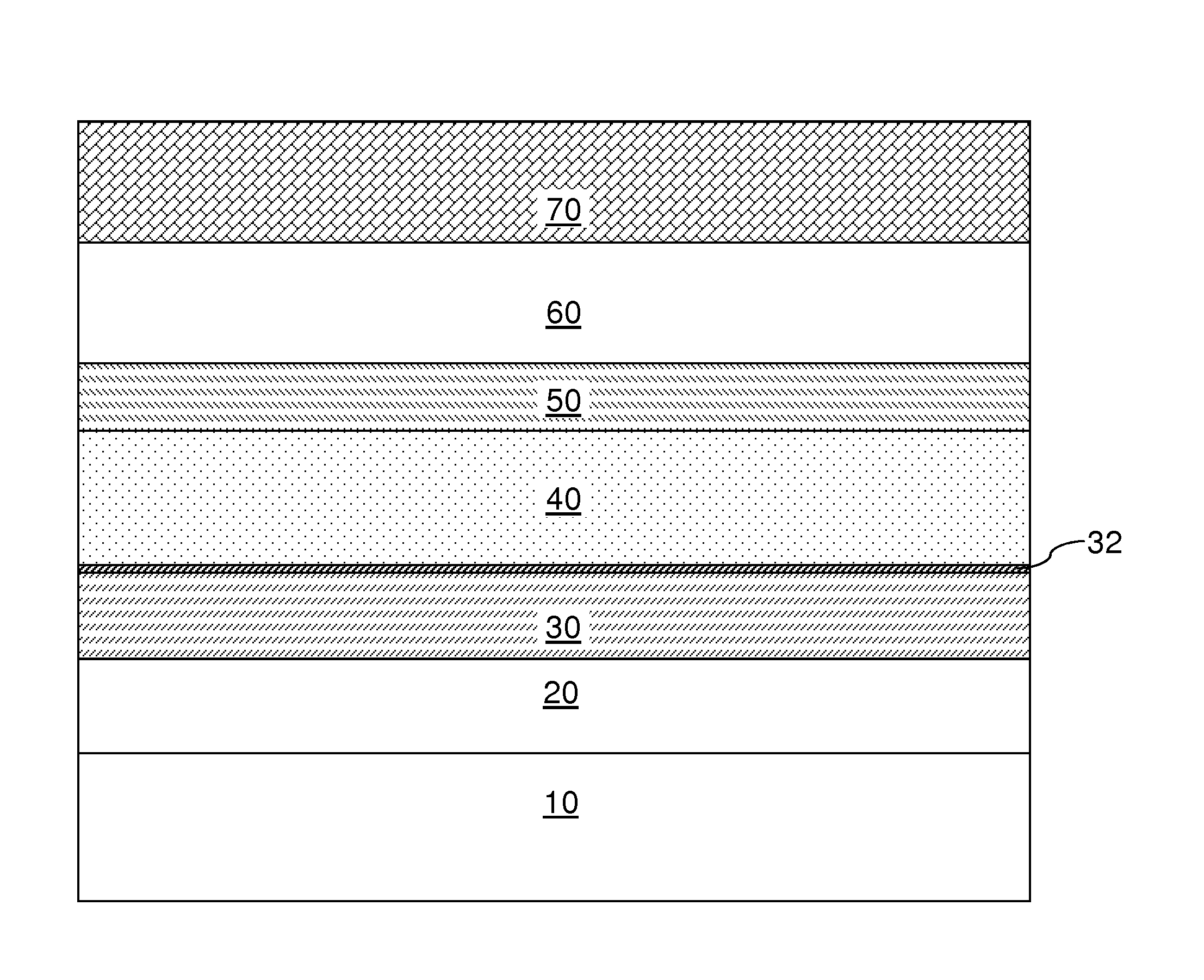
[0017]As stated above, the present disclosure relates to a plasma treatment process applied at a p-i junction for increasing open circuit voltage of a photovoltaic device and a photovoltaic device thereby formed and including an interfacial nanocrystalline layer, which are now described in detail with accompanying figures. Throughout the drawings, the same reference numerals or letters are used to designate like or equivalent elements. The drawings are not necessarily drawn to scale.
[0018]As used herein, a crystal structure is “nanocrystalline” if the average grain size of the material is from 1 nm to 1 micron.
[0019]As used herein, a “silicon-containing semiconductor” or a “silicon-containing semiconductor material” is a semiconductor material that includes silicon.
[0020]As used herein, a “silicon-containing reactant gas” is a gas that includes at least one silicon atom in a molecule thereof and is capable of depositing silicon under suitable process conditions. Non-limiting example...
PUM
| Property | Measurement | Unit |
|---|---|---|
| open circuit voltage | aaaaa | aaaaa |
| thickness | aaaaa | aaaaa |
| thickness | aaaaa | aaaaa |
Abstract
Description
Claims
Application Information