

Sensitivity sensor system
- Summary
- Abstract
- Description
- Claims
- Application Information
AI Technical Summary
Benefits of technology
Problems solved by technology
Method used
Image

Examples
first embodiment
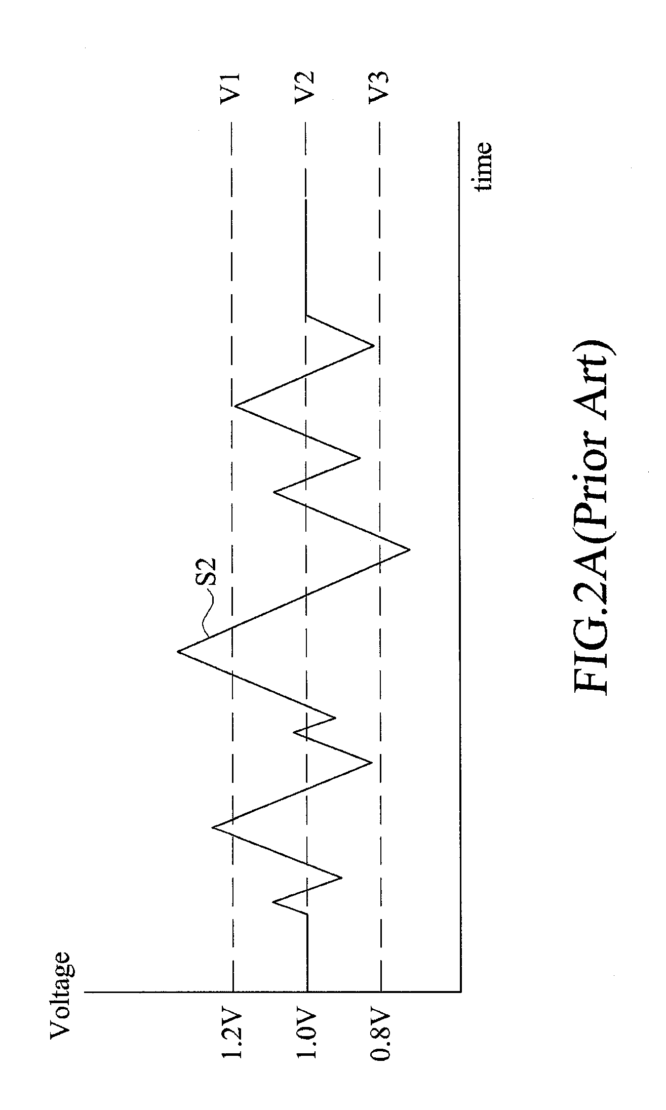
[0059]FIG. 6A shows a voltage-time graph of the first embodiment when the normalized signal S5 in the sensor system of the present invention is at a predetermined sensitivity. Also refer to FIG. 4 and as illustrated, when the first and second comparison voltages V4 and V6 and the reference voltage V5 are at 1.2 volts, 0.8 volt and 1 volt respectively. Under this condition, the first and second comparison voltages V4 and V6 cooperatively define the standby voltage region of 0.4 volt. Therefore, as shown in FIG. 6A, the fluctuation bias voltage of the normalized signal S5 is located outside of the standby voltage region defined cooperatively by the first and second comparison voltages V4 and V6 three times. Thus, the triggering signal S6 is generated three times.
[0060]FIG. 6B shows the voltage-time graph of the first embodiment after lowering the sensitivity of the normalized signal in the sensor system of the present invention. Also refer to FIG. 4 and as illustrated, when it is desi...
third embodiment
[0067]FIG. 7 shows a circuit diagram employed in third embodiment of the sensor system of the present invention. The divider circuit 31 preferably includes three resistors R5 and R6 and R7. The DAC (digital / analog converter) 34 has one input end coupled electrically to the electronic device in order to the electronic devices delivers the digital control signal S4 to the DAC 34, where the digital control signal S4 is converted into the analog control signal S4′. The DAC 34 has an output end coupled electrically to a first end of the resistor R5 while a second end of the resistor R5 is coupled electrically to a first end of the resistor R6. The resistor R6 has a second end coupled electrically to a first end of the resistor R7. The resistor R7 has a second end coupled electrically to the ground GND.
[0068]Note that, the adjoining point of the resistors R5 and R6 serves as a first voltage contact P4, wherein the analog control signal S4′ after passing through the resistor R5 and drops i...
fourth embodiment
[0076]FIG. 9 shows a circuit diagram employed in the sensor system of the present invention. As illustrated, the divider circuit 31 preferably includes three resistors R6, R7, R8. The DAC (digital / analog converter) 34 has an input end coupled electrically to the electronic device in order to enable electronic device delivers the digital control signal S4 into the DAC (digital / analog converter) 34, where the digital control signal S4 is converted into the analog control signal S4′. The DAC (digital / analog converter) 34 has an output end coupled electrically to a first end of the resistor R6 while a second end of the resistor R6 is coupled electrically to a first end of the resistor R7, which has a second end coupled electrically to a first end of the resistor R8. The resistor R8 has a second end coupled electrically to the ground GND.
[0077]Note that, the adjoining point of the resistors R6 and R7 serves as the normalized voltage contact P5, wherein the analog control signal S4′ after...
PUM
 Abstract
Description
Claims
Application Information