Switching power supply device, switching power supply circuit, and electrical equipment
- Summary
- Abstract
- Description
- Claims
- Application Information
AI Technical Summary
Benefits of technology
Problems solved by technology
Method used
Image
Examples
first embodiment
[0043]First, a first embodiment is described.
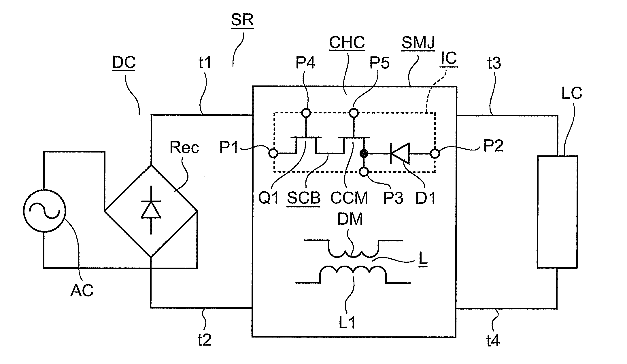
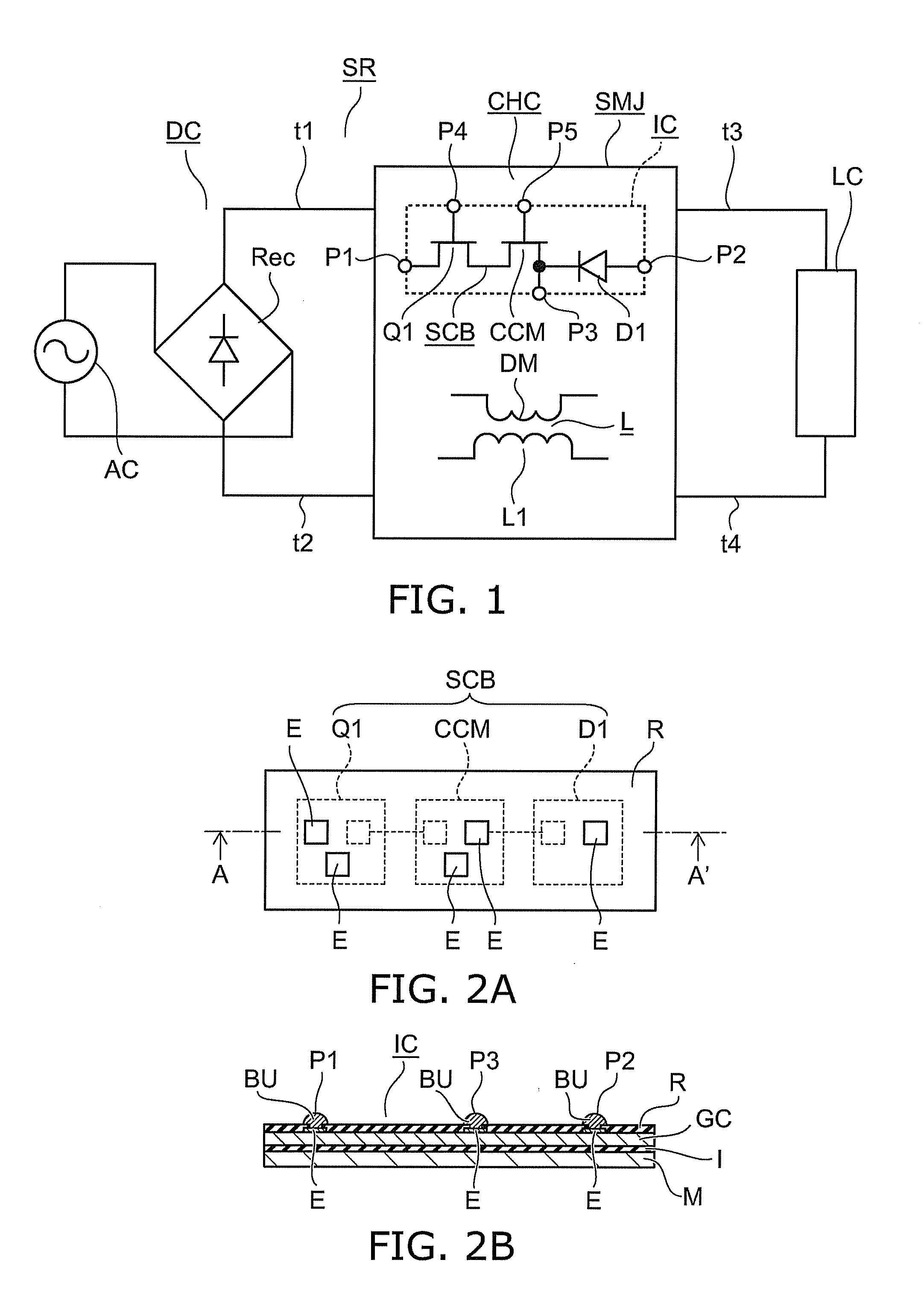
[0044]FIG. 1 is a circuit diagram illustrating a switching power supply device according to the first embodiment.
[0045]FIGS. 2A and 2B illustrate the configuration of the switching power supply device. More specifically, FIG. 2A is a schematic top view, and FIG. 2B is a sectional view taken along line A-A′ of FIG. 2A.
[0046]As shown in FIGS. 1 to 2B, the switching power supply device IC according to the first embodiment includes an integrated body SCB in which a first switching element Q1, a constant current element CCM, and a diode D1 are connected in series and integrated. Furthermore, the switching power supply device IC includes first to fifth external terminals P1-P5 as a plurality of external terminals. The first external terminal P1 is connected to the main terminal of the element disposed on one end side of the integrated body SCB. The second external terminal P2 is connected to the main terminal of the element disposed on the othe...
second embodiment
[0066]A second embodiment is described.
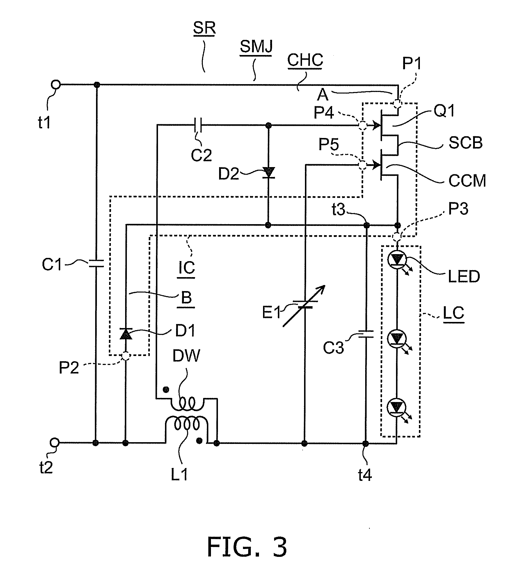
[0067]FIG. 3 is a circuit diagram illustrating a switching power supply circuit according to the second embodiment.
[0068]As shown in FIG. 3, the chopper circuit CHC is of the step-down type. For each of the first switching element Q1 and the constant current element CCM of its switching power supply device IC, for instance, a GaN-HEMT is used. The first inductor L1 is connected between the load circuit LC and the input end t2. The second inductor DW is connected between the fourth external terminal P4 and the third external terminal P3 of the switching power supply device IC through the load circuit LC and the coupling capacitor C2. That is, the second inductor DW is connected between the control terminal (gate) of the first switching element Q1 and the other main terminal (source) of the constant current element CCM.
[0069]In the switching power supply device IC, the first external terminal P1 is connected to the input end t1. The second extern...
third embodiment
[0081]Next, a third embodiment is described.
[0082]FIG. 4 is a circuit diagram illustrating a switching power supply circuit according to the third embodiment.
[0083]The switching power supply circuit SR shown in FIG. 4 is of the step-down type as in the second embodiment. However, the first inductor L1 is connected to a position between the constant current element CCM and the parallel circuit of the output capacitor C3 and the load circuit LC. The potential source E1 having adjustable potential difference is directly connected between the control terminal (gate) and the other main terminal (source) of the constant current element CCM. Furthermore, the second inductor DW is connected at its both ends between the fourth external terminal P4 and the third external terminal P3 of the switching power supply device IC through the coupling capacitor C2. In FIGS. 4 to 13 showing the fourth and subsequent embodiments, the same components as those in FIG. 3 are labeled with like reference num...
PUM
 Abstract
Description
Claims
Application Information


