Method for manufacturing semiconductor device

a manufacturing method and semiconductor technology, applied in the direction of semiconductor devices, basic electric elements, electrical appliances, etc., can solve the problems of a large tendency to crack in the separation step, achieve the effect of reducing the tendency to crack, reducing the risk of cracking, and improving the yield of semiconductor elements

Active Publication Date: 2011-12-29
SEMICON ENERGY LAB CO LTD
View PDF5 Cites 53 Cited by
  • Summary
  • Abstract
  • Description
  • Claims
  • Application Information

AI Technical Summary

Benefits of technology

[0028]According to one embodiment of the present invention, formation of a crack suppression layer formed of a metal film or a crack suppression layer formed of a resin film makes it possible to suppress a crack occurring in a semiconductor element when the semiconductor element is separated from a substrate. Thus, yield in manufacturing the semiconductor element can be improved.
[0029]According to one embodiment of the present invention, a crack suppression layer formed of a metal film can be formed using the same material as at least one of a gate electrode layer, a source electrode layer, and a drain electrode layer of a semiconductor element, so that the crack suppression layer formed of a metal film can be easily formed without increasing the number of manufacturing steps.
[0030]According to one embodiment of the present invention, a crack suppression layer formed of a resin film can be formed using the same material as at least one of an insulating layer, a protective insulating layer, and a partition of a semiconductor element, so that the crack suppression layer formed of a resin film can be easily formed without increasing the number of manufacturing steps.
[0031]According to one embodiment of the present invention, a crack caused in a separation step tends to occur from the periphery of a substrate, and also tends to occur in a resin film having a low mechanical strength. Thus, with a metal film having a high mechanical strength, a crack can be suppressed. A crack occurs and grows in a resin film which is formed continuously over a plane; however, if a resin film is formed discontinuously and has a higher mechanical strength than the resin film in which the crack occurs, a crack can be suppressed.
[0032]Therefore, even in a situation where occurrence of a crack in a separation step is unavoidable, if a crack suppression layer formed of a metal film or a crack suppression layer formed of a resin film is formed in the periphery of a desired semiconductor element, progression (growth) of a crack can be suppressed by the crack suppression layer, so that yield in manufacturing a semiconductor element can be improved.

Problems solved by technology

When the bending stress is applied to the semiconductor elements, breaking or a crack easily occurs in the layer to be separated, which causes malfunctions such as breaking of the semiconductor devices.
A crack caused in a separation step tends to occur from the periphery of a substrate.

Method used


Image

  • Method for manufacturing semiconductor device
  • Method for manufacturing semiconductor device
  • Method for manufacturing semiconductor device

Examples


embodiment 1

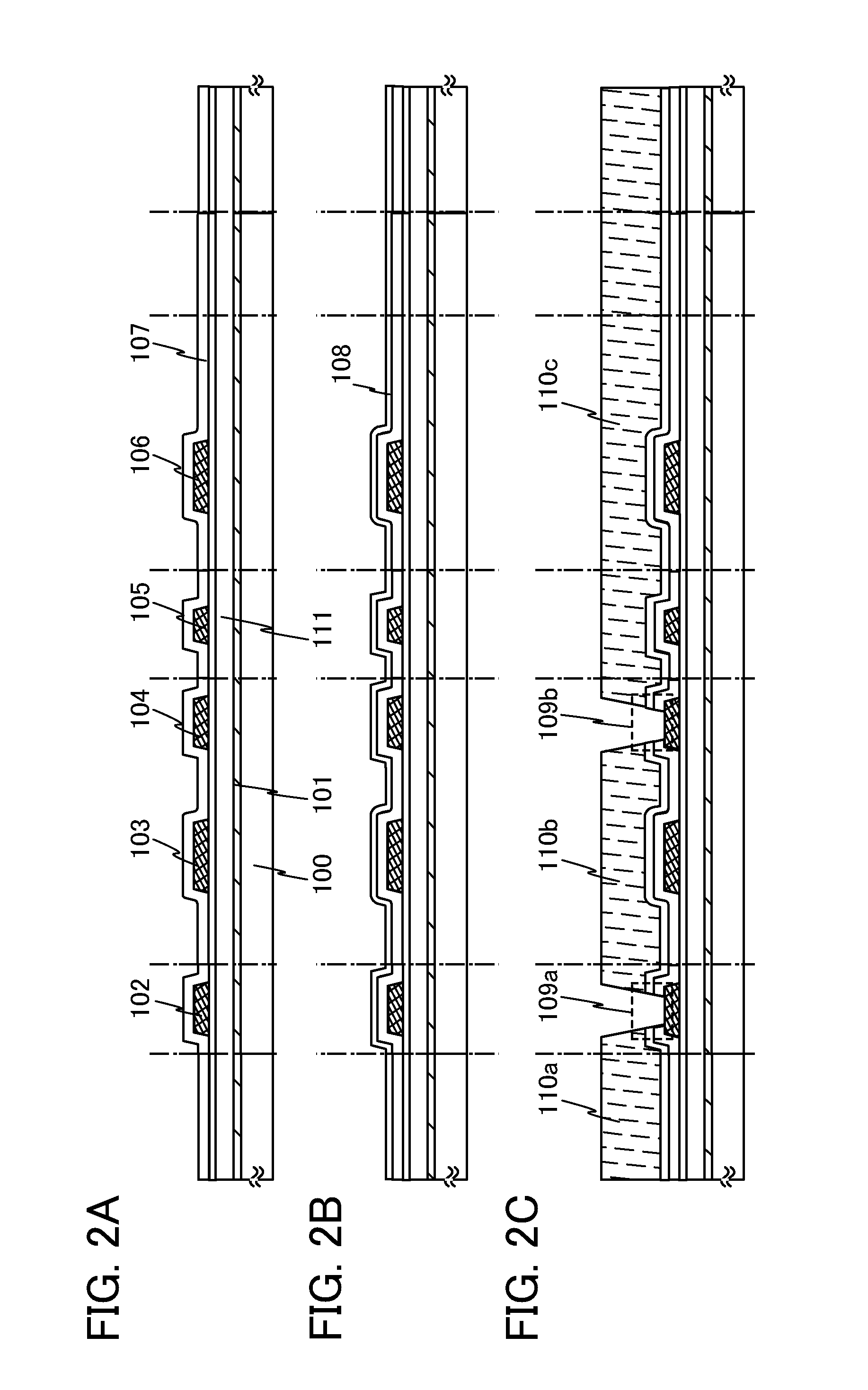
[0051]In this embodiment, a manufacturing process of a semiconductor device will be described with reference to FIGS. 1A and 1B, FIGS. 2A to 2C, FIGS. 3A to 3C, FIGS. 4A and 4B, FIGS. 5A and 5B, FIG. 6, FIGS. 7A and 7B, FIGS. 8A and 8B, and FIG. 9.

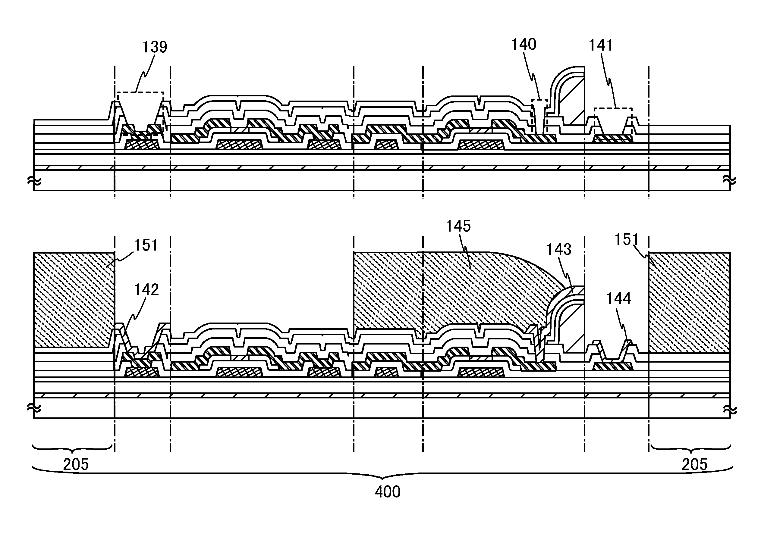
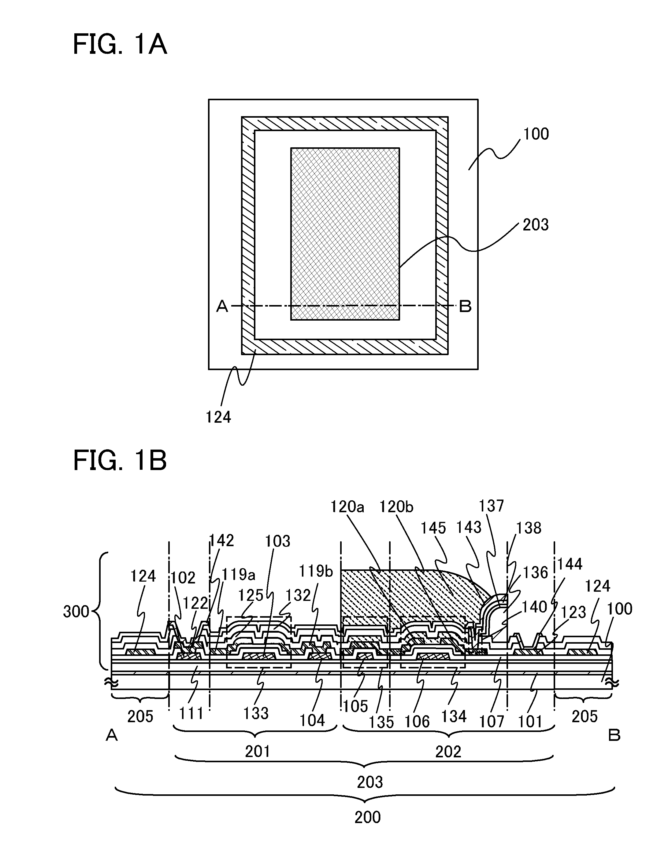
[0052]FIG. 1A is a planar view of a semiconductor device, and FIG. 1B is a cross-sectional view along a dashed line A-B in FIG. 1A. Note that FIGS. 1A and 1B are a planar view and a cross-sectional view showing a state where a manufacturing process of a semiconductor element is completed and before the semiconductor element is separated from a first substrate.

[0053]A semiconductor device 200 in FIGS. 1A and 1B includes a separation layer 101 over a first substrate 100, a first insulating layer 111 over the separation layer 101, a transistor 134 included in a pixel circuit portion 202 and a transistor 133 included in a driver circuit portion 201 over the first insulating layer 111, and a crack suppression region 205 including a crack suppre...

embodiment 2

[0187]This embodiment shows an example of forming a crack suppression layer formed of a resin layer, which is different from the crack suppression layer formed of a metal film in Embodiment 1, with reference to FIGS. 14A and 14B, FIGS. 15A and 15B, and FIGS. 16A and 16B. Therefore, part of this embodiment can be performed in a manner similar to that of Embodiment 1; thus, repetitive description of the same portions as or portions having functions similar to those in Embodiment 1 and steps for forming such portions will be omitted. Since FIGS. 14A and 14B, FIGS. 15A and 15B, and FIGS. 16A and 16B are the same as FIGS. 1A and 1B, FIGS. 2A to 2C, FIGS. 3A to 3C, FIGS. 4A and 4B, FIGS. 5A and 5B, FIG. 6, FIGS. 7A and 7B, FIGS. 8A and 8B, and FIG. 9 except for part of steps, the same portions are denoted by the same reference numerals and detailed description thereof will not be repeated.

[0188]First, in accordance with Embodiment 1, the separation layer 101, the first insulating layer 11...

embodiment 3

[0225]In this embodiment, a method for manufacturing a semiconductor device which is different from those of the above embodiments will be described with reference to FIGS. 10A to 10C, FIGS. 11A to 11C, FIGS. 12A to 12C, and FIG. 13. In each of Embodiments 1 and 2, a method for manufacturing a display device which is one of semiconductor devices including a transistor included in a driver circuit portion and a pixel circuit portion is described, while in this embodiment, a method for manufacturing a semiconductor integrated circuit chip (also referred to as an IC chip) which is another embodiment of a semiconductor device will be described.

[0226]FIG. 10A is a planar view of a semiconductor device. FIG. 10B shows an enlarged planar view of one piece of the semiconductor integrated circuit chip which is the semiconductor device in FIG. 10A. FIG. 10C is a cross-sectional view taken along a broken line C-D in FIG. 10B. Note that FIGS. 10A to 10C are planar views and a cross-sectional vi...


PUM


Abstract

An object is to provide a manufacturing method of a semiconductor device in which a defect in characteristics due to a crack occurring in a semiconductor device is reduced. Provision of a crack suppression layer formed of a metal film in the periphery of a semiconductor element makes it possible to suppress a crack occurring from the outer periphery of a substrate and reduce damage to the semiconductor element. In addition, even if the semiconductor device is subjected to physical forces from the outer periphery in separation and transposition steps, progression (growth) of a crack to the semiconductor device can be suppressed by the crack suppression layer.

Description

BACKGROUND OF THE INVENTION[0001]1. Field of the Invention[0002]The present invention relates to a method for manufacturing a semiconductor device.[0003]Note that in this specification, the term “semiconductor device” refers to general devices that can function by utilizing semiconductor properties, and substrates over which semiconductor elements such as thin film transistors (TFTs) are formed, liquid crystal display devices driven using TFTs, electroluminescence (EL) display devices driven using TFTs, semiconductor circuits, and electronic devices are all defined as semiconductor devices.[0004]2. Description of the Related Art[0005]In recent years, techniques of manufacturing semiconductor devices have been greatly improved: flexible substrates are capable of reducing size and weight of semiconductor devices, and further achieving flexibility and impact resistance of semiconductor devices, and thus, are considered to be used for semiconductor devices.[0006]As a method for manufact...

Claims


Application Information

Patent Timeline
Patent Type & Authority Applications(United States)
IPC IPC(8): H01L21/336H01L21/20
CPCH01L21/02554H01L21/02565H01L21/02631H01L2227/326H01L27/1266H01L2227/323H01L27/1225H10K71/80H10K59/1201H01L27/1218H01L27/1244
Inventor CHIDA, AKIHIRO
Owner SEMICON ENERGY LAB CO LTD
Why Eureka
Try Eureka