Substrate processing method

a processing method and substrate technology, applied in plasma technique, electrical equipment, electric discharge tubes, etc., can solve the problems of reducing the etching efficiency of positive ions, and achieve the effect of preventing the etching efficiency reduction by positive ions and increasing the overall etching efficiency

Active Publication Date: 2011-12-29
TOKYO ELECTRON LTD
View PDF6 Cites 14 Cited by
  • Summary
  • Abstract
  • Description
  • Claims
  • Application Information

AI Technical Summary

Benefits of technology

[0016]In accordance with the present disclosure, since the duty ratio of the high frequency power for biasing is greater than that of the high frequency power for plasma generation, the negative ion attraction process can be performed after performing the positive ion etching process for enough time. Thus, the decrease in the etching efficiency by the positive ions may be prevented and the overall etching efficiency can be increased by effectively using the negative ions.

Problems solved by technology

Accordingly, the hole 71 is deformed, which results in the decrease in the etching efficiency by the positive ions.

Method used


Image

  • Substrate processing method
  • Substrate processing method
  • Substrate processing method

Examples


Embodiment Construction

[0025]Hereinafter, embodiments of the present disclosure will be described in detail with reference to the accompanying drawings.

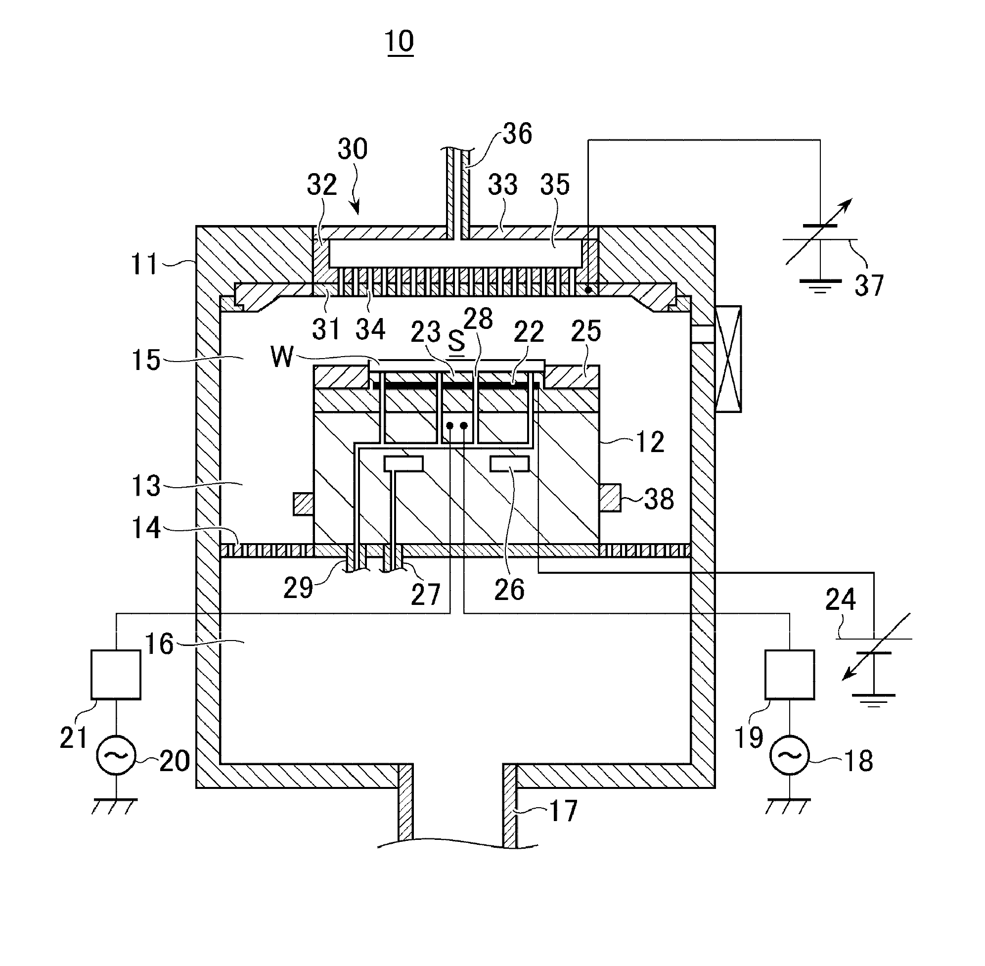
[0026]FIG. 1 is a cross sectional view showing a schematic configuration of a substrate processing apparatus for performing a substrate processing method in accordance with an embodiment of the present disclosure. The substrate processing apparatus performs a predetermined plasma etching process on a substrate.

[0027]In FIG. 1, the substrate processing apparatus 10 includes a chamber 11 for accommodating therein a semiconductor wafer W (hereinafter, referred to as “wafer”), and a cylindrical susceptor 12 for mounting thereon the wafer W is installed within the chamber 11. A side exhaust path 13 is formed by an inner sidewall of the chamber 11 and a side surface of the susceptor 12. A gas exhaust plate 14 is installed on the way of the side exhaust path 13.

[0028]The gas exhaust plate 14 is a plate-shaped member having a multiple number of through holes and s...


PUM


Abstract

There is provided a substrate processing method capable of preventing the decrease in etching efficiency by positive ions and increasing the overall etching efficiency by using negative ions. The substrate processing method includes applying a plasma RF and a bias RF in the pattern of a pulse wave, respectively. The substrate processing method repeatedly performs the steps of: (3b) etching a substrate by positive ions in plasma by applying both the plasma RF and the bias RF; (3c) generating negative ions in a processing chamber by stopping the application of both the plasma RF and the bias RF; and (3a) attracting the negative ions to the substrate by applying the bias RF and stopping the application of the plasma RF. A duty ratio of the bias RF is set to be greater than a duty ratio of the plasma RF.

Description

CROSS-REFERENCE TO RELATED APPLICATION[0001]This application claims the benefit of Japanese Patent Application No. 2010-142740 filed on Jun. 23, 2010, and U.S. Provisional Application Ser. No. 61 / 365,591 filed on Jul. 19, 2010, the entire disclosures of which are incorporated herein by reference.FIELD OF THE INVENTION[0002]The present disclosure relates to a substrate processing method for generating a plasma by applying a high frequency power for plasma generation and a high frequency power for biasing in a pattern of a pulse wave and for performing a predetermined etching process on a substrate by using the plasma.BACKGROUND OF THE INVENTION[0003]When a wiring process or the like is performed on a substrate such as a semiconductor wafer, it is required to perform a fine process on the substrate and, thus, a substrate processing method using a plasma has been widely employed.[0004]This substrate processing method uses a technique for generating a plasma in a pattern of a pulse wave...

Claims


Application Information

Patent Timeline
Patent Type & Authority Applications(United States)
IPC IPC(8): H01L21/3065
CPCH01J37/32091H01J37/32146H01L21/6719H01L21/3065H01J37/32165H01L21/02H01L21/203H01L21/205H01L21/302H01L21/30621H01L21/324H01L21/76825H01L21/76826H05H1/46
Inventor YATSUDA, KOICHIMOCHIKI, HIROMASA
Owner TOKYO ELECTRON LTD
Why Eureka
Try Eureka