Integrated capacitors fabricated with conductive metal oxides

a technology of integrated capacitors and metal oxides, which is applied in the direction of coatings, transistors, chemical vapor deposition coatings, etc., can solve the problems of difficult integration of these materials into the fabrication process flow, surrounding materials are subject to degradation, and surrounding oxidizable materials, including the polysilicon plug and the silicon substrate below, are still subject to degradation, etc., to achieve the effect of improving the uniformity and reliability of the capacitor and facilitating integration

Inactive Publication Date: 2005-09-06
MICRON TECH INC
View PDF19 Cites 9 Cited by
  • Summary
  • Abstract
  • Description
  • Claims
  • Application Information

AI Technical Summary

Benefits of technology

[0017]One object of the current invention is to provide a new process of fabricating a bottom electrode for an integrated capacitor with a more conformal structure, thereby improving the uniformity and reliability of the capacitor, and also the process window to facilitate integration.
[0018]Another objective is to increase the etching efficiency during patterning of a conductive oxide film, particularly by polishing processes.
[0019]Another objective is to provide a structure of a container capacitor with a lower electrode plate having less sharp corners, to improve the reliability and decrease the leakage of the capacitor.
[0020]In order to achieve the above objectives, the preferred embodiments focus on an improved film deposition process and a film crystallization process for a conductive oxide film. Desirably, the process deposits a metal oxide film, in the preferred embodiment RuOx, under a relatively low temperature, such as will produce an amorphous film. As a result, the metal oxide film is more conformally deposited over a three-dimensional folding structure, uniformly covering the structure. Furthermore, since the amorphous metal oxide film is much softer compared to the crystallized film, subsequent patterning steps can be more efficient so as to increase the manufacturing efficiency and throughput.
[0021]In order to increase the conductivity of the metal oxide films, a post-deposition high temperature anneal crystallizes the metal oxide film, desirably in a non-oxidizing ambient. Preferably, this annealing process is conducted after the CMP polishing. As mentioned earlier, the metal oxide film is easier to etch, and particularly easier to polish, in an amorphous state. Moreover, the rim or edge area of the metal oxide film that serves as a bottom electrode plate of the capacitor is made less sharp due to a more conformal deposition. Consequently, the formation of more rounded corners of the bottom electrode plate reduces field strength and the risk of current leakage during operation of the circuit.

Problems solved by technology

Difficulties have been encountered, however, in incorporating these materials into fabrication process flows.
Due to the volatility of the reactants and by-products of processes for forming high k materials, surrounding materials are subject to degradation.
Therefore, the surrounding oxidizable materials, including the polysilicon plug and the silicon substrate below, are still subject to degradation.
Oxidation of the electrode, the underlying polysilicon plug or the underlying substrate reduces conductivity of these electrical elements, while oxidation of electrode surfaces adjacent the dielectric reduces cell capacitance due to the formation of a layer of oxide with a relatively low dielectric constant.
These problems have been viewed as major obstacles to incorporating high k materials into integrated circuits.
However, existing processes for fabricating RuOx / high-k container capacitors with the structure of FIG. 1 has some disadvantages. FIGS. 2A-2D illustrate conventional process steps, and, for the purpose of simplicity, the drawings only show the capacitor container without showing the underlying devices, such as the substrate, the transistors and the conductive plugs.
This undesirable configuration will often cause discontinuities in the film 214.
Thus, the process margin is limited, especially for circuit designs in which conformal dielectrics are needed.
The CMP process, however, can not be efficiently carried out due to the extreme hardness of the crystallized RuOx film 214.
The difficulty of the CMP adversely affects the throughput of the fabrication.
Thus, when the next layer of a high-k dielectric material 216 is deposited, as shown in FIG. 2C, the non-ideal conformality of the structure can cause a fatal defect of the device, especially at the thinning point 224.
If the dielectric layer is too thin at this point, the capacitor can be leaky, or even shorted.
Again, due to imperfect conformality in the previously formed dielectric, there may be a void left inside the container.
As is known in the art, such voids can trap moisture and thereby reduce device lifespan.

Method used


Image

  • Integrated capacitors fabricated with conductive metal oxides
  • Integrated capacitors fabricated with conductive metal oxides
  • Integrated capacitors fabricated with conductive metal oxides

Examples


Embodiment Construction

[0029]Although the present invention is described in the context of fabricating memory devices, those skilled in the art of integrated capacitor fabrication will readily find application for the principles disclosed herein in many other contexts.

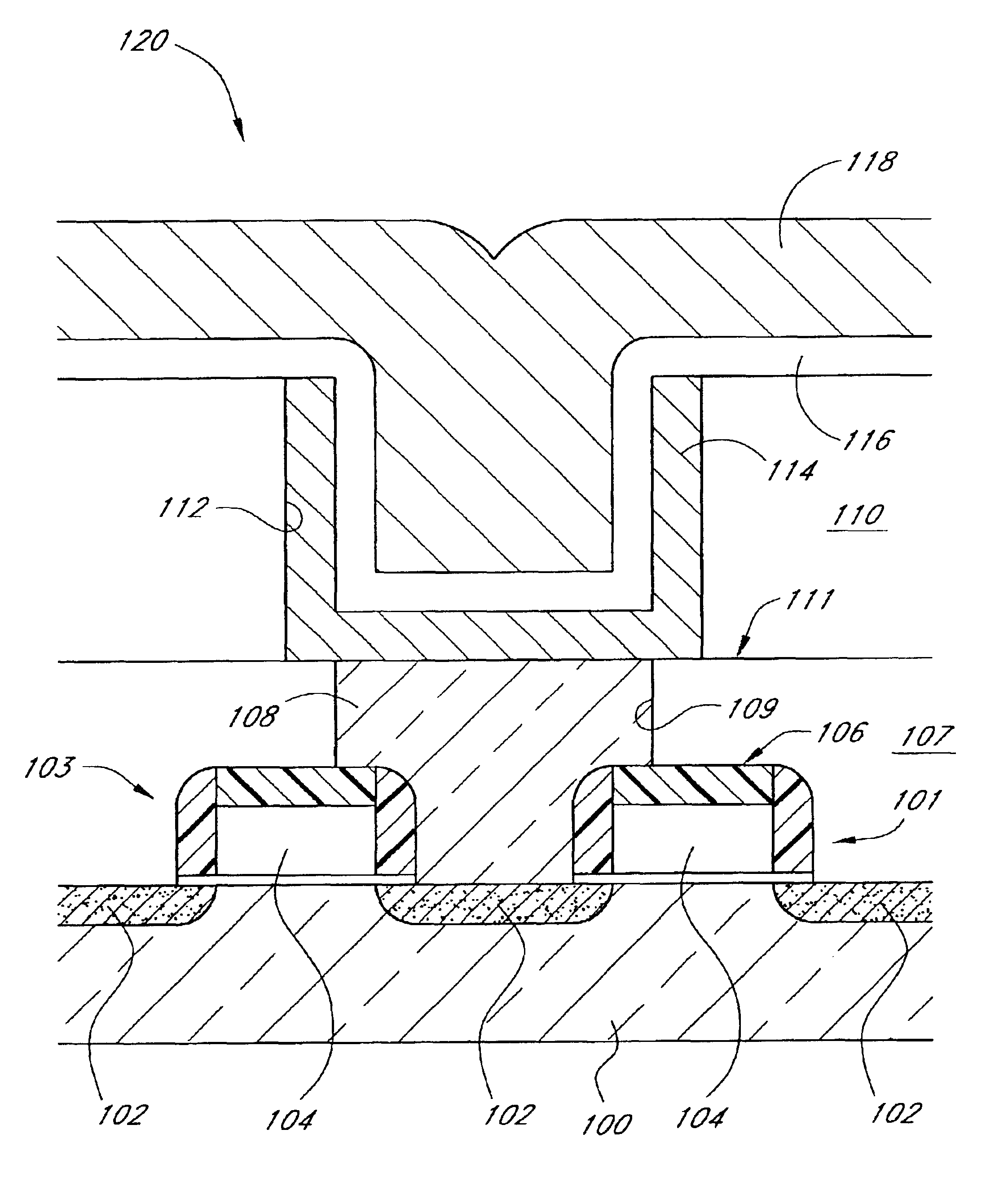
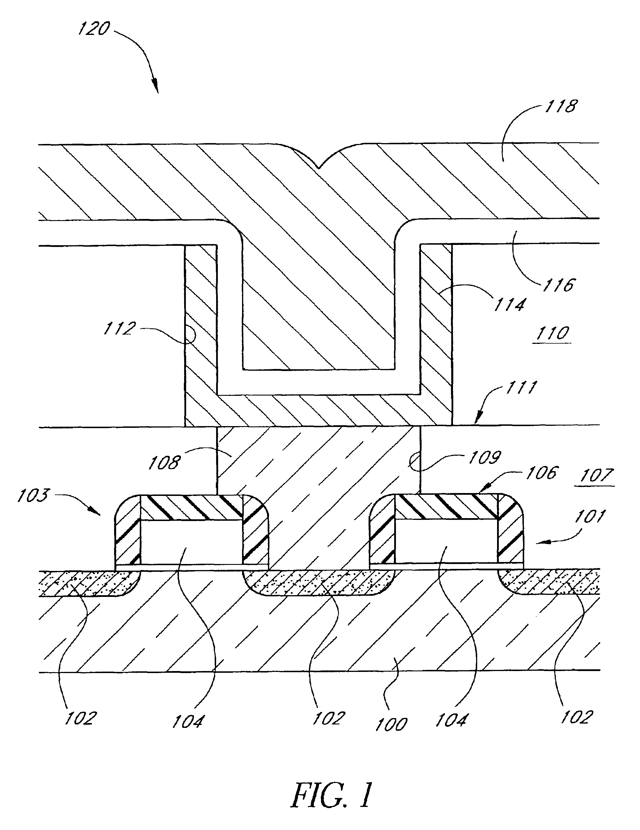
[0030]In order to understand the context in which the preferred embodiments are employed, reference is made to FIG. 1, in which a basic structure of a container capacitor is illustrated over a semiconductor substrate 100. As will be understood by the skilled artisan, the substrate 100 can comprise the upper portion of an intrinsically doped, monocrystalline silicon wafer, an epitaxial semiconductor layer, or other semiconductor material in which the lowest level of devices are formed.

[0031]As shown in FIG. 1, a plurality of transistors 101, 103 is fabricated in and above the substrate 100, and a first layer of insulating or dielectric material 107 is formed thereover. Generally, this insulating layer 107 comprises a form of oxide, such as bo...


PUM

PropertyMeasurementUnit
dielectric constantaaaaaaaaaa

Abstract

A capacitor for a memory device is formed with a conductive oxide for a bottom electrode. The conductive oxide (RuOx) is deposited under low temperatures as an amorphous film. As a result, the film is conformally deposited over a three dimensional, folding structure. Furthermore, a subsequent polishing step is easily performed on the amorphous film, increasing wafer throughput. After deposition and polishing, the film is crystallized in a non-oxidizing ambient.

Description

REFERENCE TO RELATED APPLICATION[0001]The present application is a divisional of U.S. application Ser. No. 09 / 546,492, filed Apr. 10, 2000 now U.S. Pat. No. 6,492,241.FIELD OF THE INVENTION[0002]The present invention relates to integrated semiconductor memory cell capacitors. In particular, the present invention relates to a memory cell capacitor fabricated with conductive metal oxides and high dielectric constant materials and a method for manufacturing such a capacitor.BACKGROUND OF THE INVENTION[0003]A memory cell in an integrated circuit, such as a dynamic random access memory (DRAM) array, typically comprises a charge storage capacitor (or cell capacitor) coupled to an access device, such as a Metal-Oxide-Semiconductor Field Effect Transistor (MOSFET). The MOSFET functions to either apply or remove charge on the capacitor, thus affecting a logical state defined by the stored charge. The amount of charge stored on the capacitor is proportional to the capacitance, C=kk0A / d, where...

Claims


Application Information

Patent Timeline
Patent Type & Authority Patents(United States)
IPC IPC(8): C23C16/40H01L21/02
CPCC23C16/40H01L28/60H01L28/55H01L28/90
Inventor RHODES, HOWARD E.VISOKAY, MARKGRAETTINGER, TOMGEALY, DANSANDHU, GURTEJBASCERI, CEMCUMMINGS, STEVE
Owner MICRON TECH INC
Why Eureka
Try Eureka