Parellel optical transceiver module

a transceiver module and parallel technology, applied in the field of data processing systems, can solve the problems of complex and costly optical modules, limited high speed performance, and complex and costly existing packaging solutions

Active Publication Date: 2012-01-05
GLOBALFOUNDRIES US INC
View PDF1 Cites 98 Cited by
  • Summary
  • Abstract
  • Description
  • Claims
  • Application Information

AI Technical Summary

Problems solved by technology

The current packaging of parallel optical transmitter, receiver, and transceiver modules typically requires multiple levels of packaging, which results in complex and costly optical modules.
As a result, existing packaging solutions may be complex, costly, and limited in high speed performance due to electrical packaging parasitics.

Method used


Image

  • Parellel optical transceiver module
  • Parellel optical transceiver module
  • Parellel optical transceiver module

Examples


Embodiment Construction

[0014]With reference now to the figures, and in particular, with reference to FIGS. 1-4, diagrams of apparatuses are provided in which illustrative embodiments may be implemented. It should be appreciated that FIGS. 1-4 are only meant as examples and are not intended to assert or imply any limitation with regard to the apparatuses in which different embodiments may be implemented. Many modifications to the depicted apparatuses may be made.

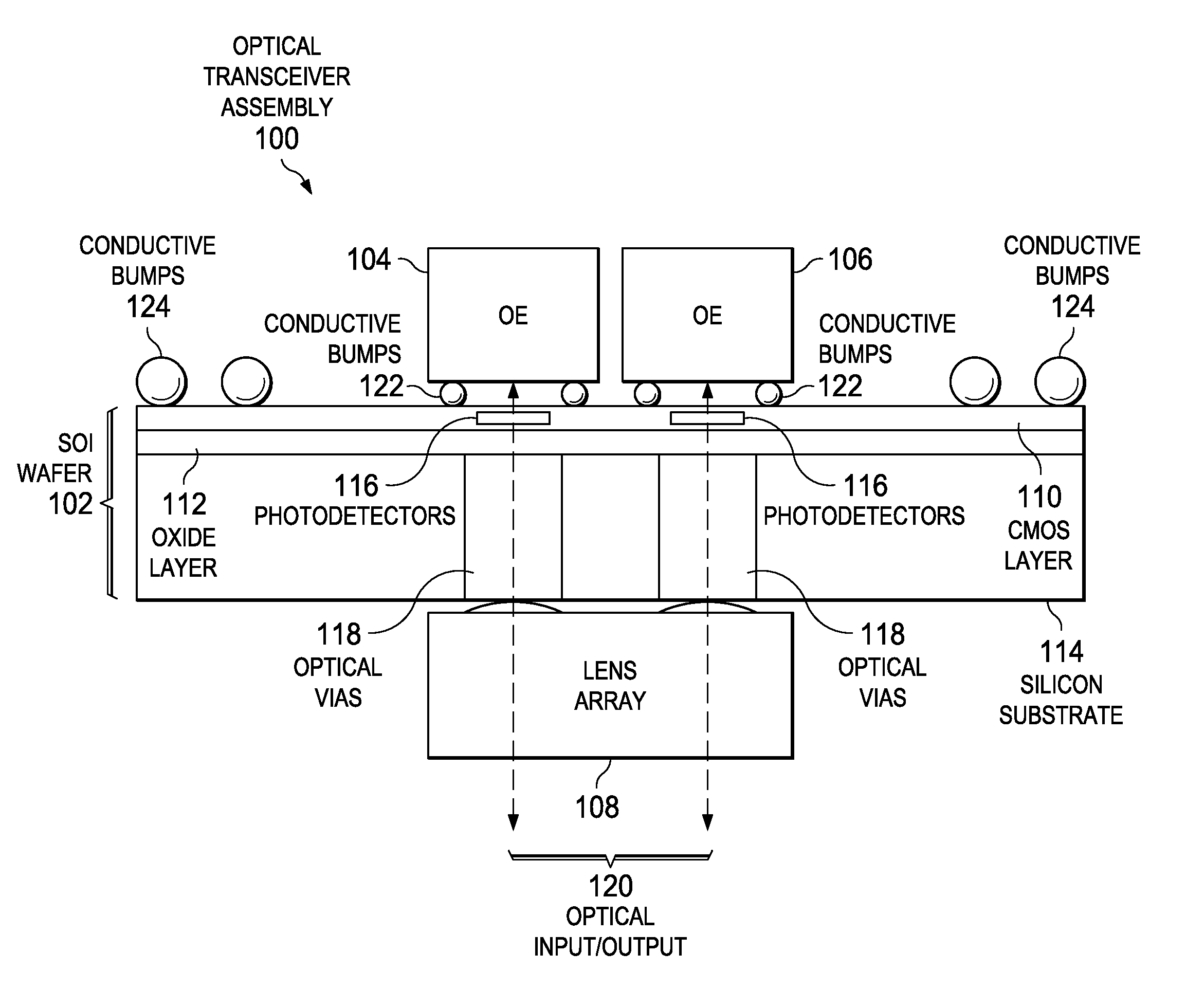
[0015]FIG. 1 depicts a diagram of a cross-section view of an optical transceiver assembly in accordance with an illustrative embodiment. Optical transceiver assembly 100 is an electrical and optical component that is capable of transmitting and receiving pulses of light, which are used to communicate data. Optical transceiver assembly 100 includes silicon-on-insulator (SOI) wafer 102, optoelectronic device 104, optoelectronic device 106, and lens array 108.

[0016]Silicon-on-insulator wafer 102 is an example of a semiconductor chip that may be used i...


PUM


Abstract

A silicon-on-insulator wafer is provided. The silicon-on-insulator wafer includes a silicon substrate having optical vias formed therein. In addition, an optically transparent oxide layer is disposed on the silicon substrate and the optically transparent oxide layer is in contact with the optical vias. Then, a complementary metal-oxide-semiconductor layer is formed over the optically transparent oxide layer.

Description

[0001]This invention was made with Government support under Contract No.: H98230-07-C-0409 awarded by National Security Agency. The Government has certain rights in this invention.BACKGROUND[0002]1. Field[0003]The disclosure relates generally to an improved data processing system, and more specifically, to a parallel optical transceiver module using a complimentary metal-oxide-semiconductor chip with backside optical vias.[0004]2. Description of the Related Art[0005]Currently, commercial parallel optical modules are based on industry-standard 850 nanometer (nm) wavelength vertical cavity surface emitting laser (VCSEL) and photodiode optoelectronic (OE) devices. Typically, arrays of these optoelectronic devices are fabricated on a semiconductor substrate, such as gallium arsenide (GaAs) or indium phosphide (InP). Optical input and output is directed to and from the top surface of the semiconductor substrate because gallium arsenide and indium phosphide substrates are not transparent ...

Claims


Application Information

Patent Timeline
Patent Type & Authority Applications(United States)
IPC IPC(8): H01L31/0232H01L21/768
CPCG02B6/4232G02B6/4246G02B6/4249G02B6/4259G02B6/12H01L31/0203H01L27/04H01L29/02H01S5/40G02B6/4267H01L2224/16225
Inventor DOANY, FUAD E.JAHNES, CHRISTOPHER V.SCHOW, CLINT L.SOYUER, MEHMETRYLYAKOV, ALEXANDER V.
Owner GLOBALFOUNDRIES US INC
Why Eureka
Try Eureka