Semiconductor device

a semiconductor and gate technology, applied in the direction of semiconductor devices, electrical devices, transistors, etc., can solve the problems affecting the resistance value of igbt, and achieve the effects of stable main current ratio, high integration, and trivial variation in sense curren

Active Publication Date: 2012-01-12
TOYOTA JIDOSHA KK
View PDF6 Cites 15 Cited by
  • Summary
  • Abstract
  • Description
  • Claims
  • Application Information

AI Technical Summary

Benefits of technology

[0007]The present teachings were made in view of such respects. An object of the present teachings is to inhibit the variations in the sense current caused by the variations in the trench depth, and to stabilize the current detection precision.
[0009]According to the semiconductor device, for the main cell region, a trench gate type element region that is advantageous for high integration is used. Whereas, the sense cell region includes a planar gate type element region in at least a part thereof. When the planar gate type element is used, the density of carriers (holes for N type channel) per unit area becomes smaller as compared with the trench gate type element. For this reason, even when the carrier density varies, the variation in the sense current is trivial. This can stabilize the ratio of the main current flowing through the main cell region and the sense current flowing through the sense cell region. Accordingly, when the semiconductor devices are mass-produced, the detection precision of the sense cell region becomes less likely to vary.

Problems solved by technology

This results in an increase in hole density of the vicinity of the surface of the drift region (the vicinity of the surface on the body side), which affects the resistance value of the IGBT.

Method used


Image

  • Semiconductor device
  • Semiconductor device
  • Semiconductor device

Examples


embodiment 1

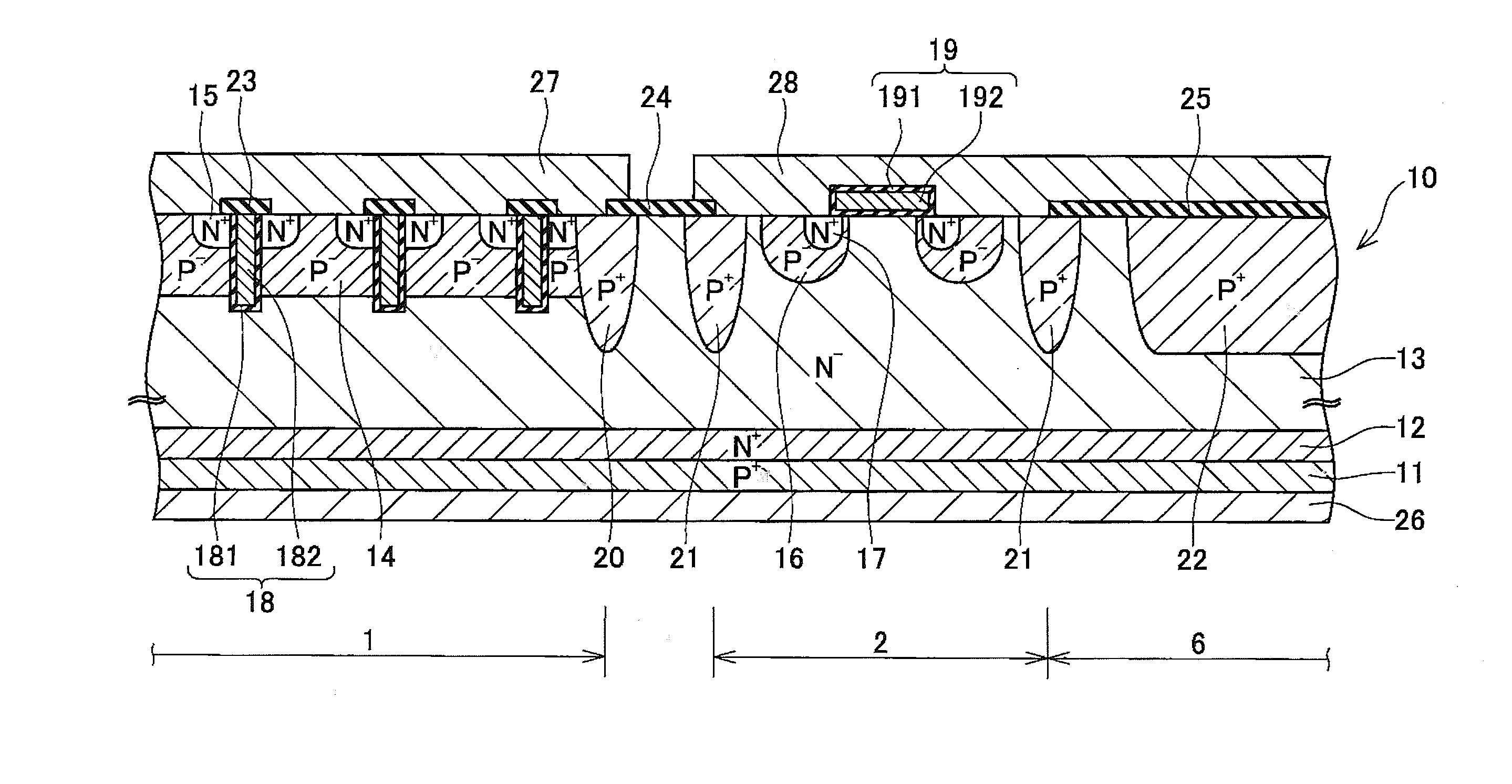
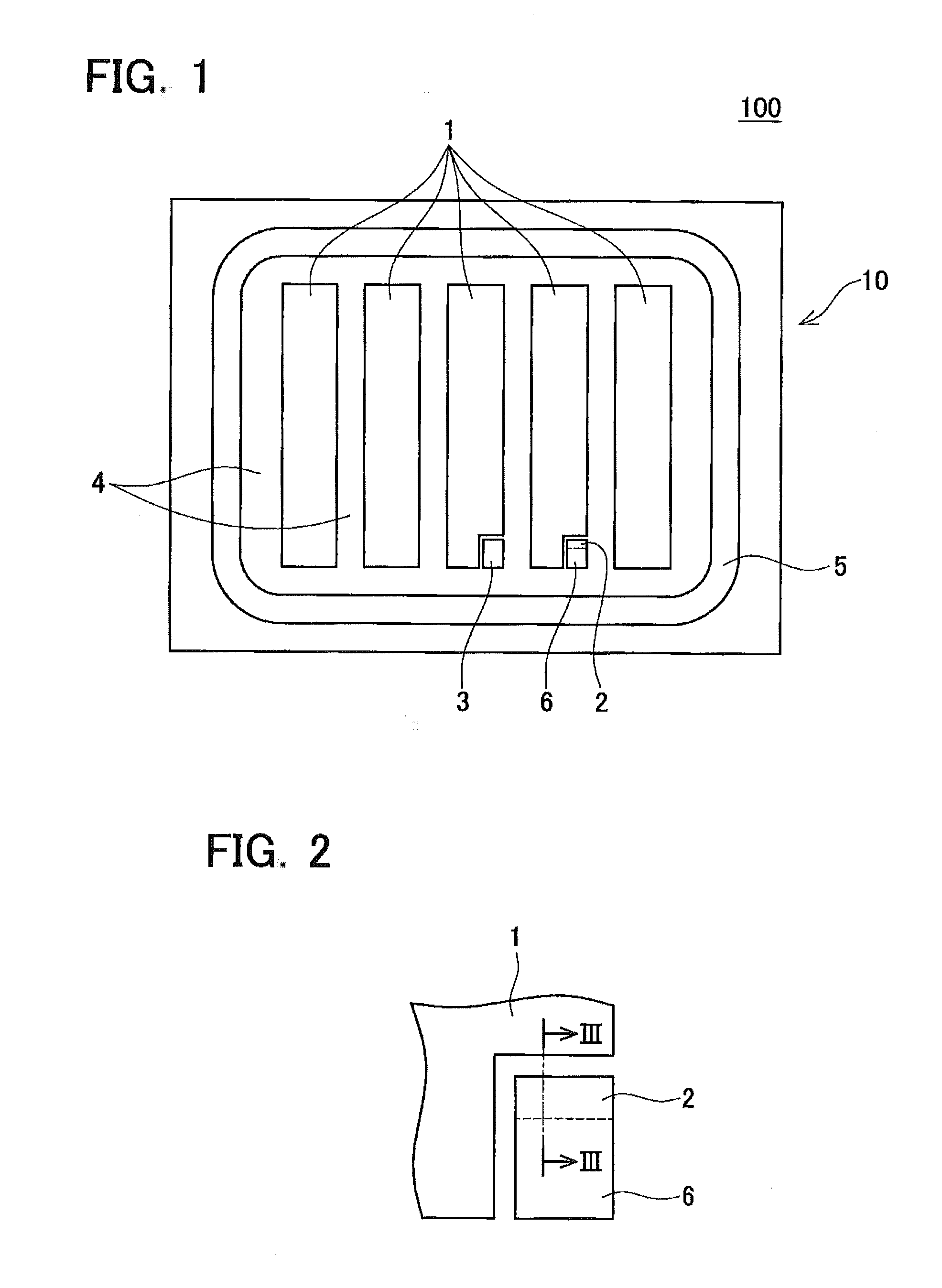
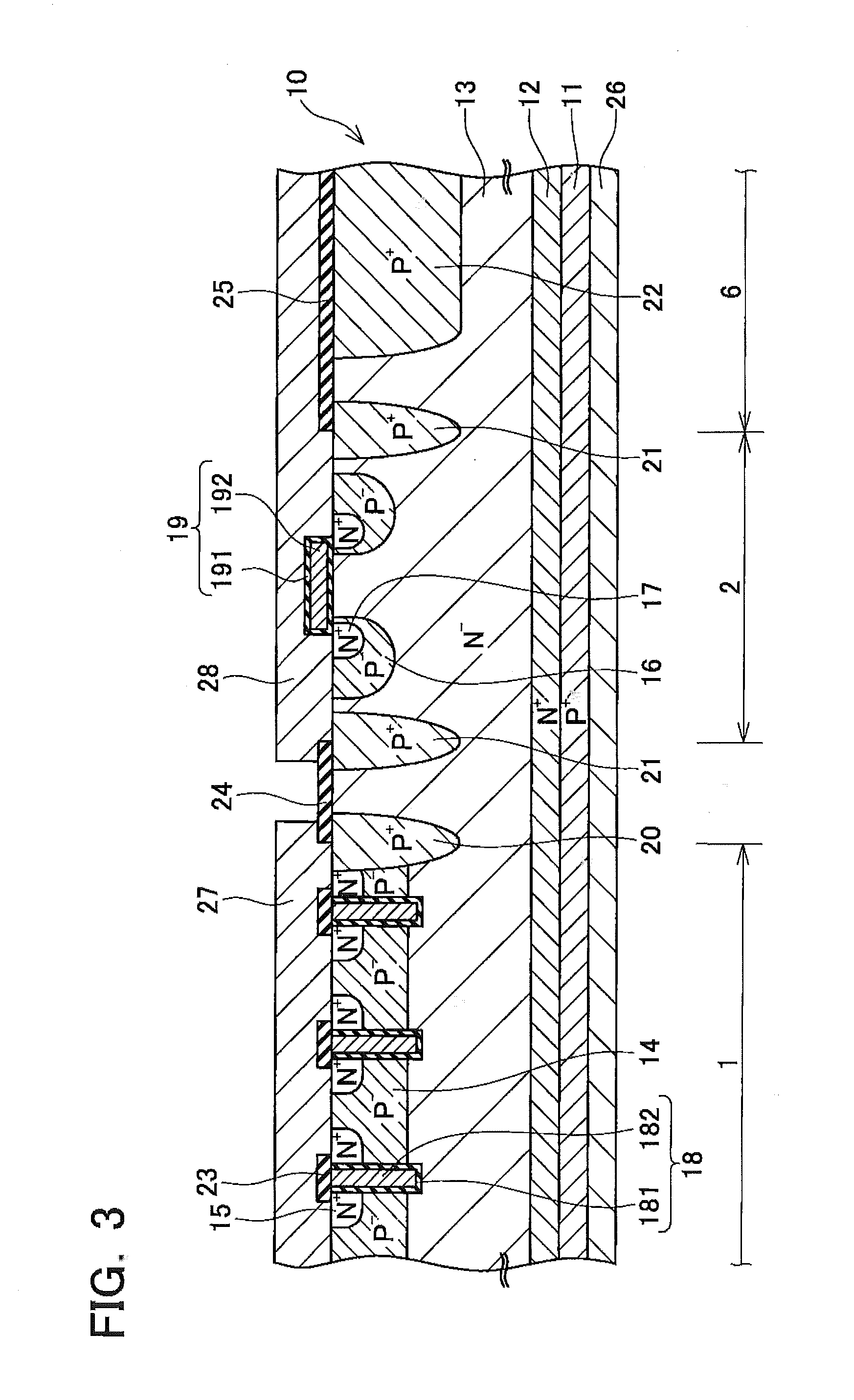
[0035]FIG. 1 is a plan view of a semiconductor device 100 in accordance with the present embodiment. FIG. 2 is an enlarged view of the vicinity of a sense cell region 2 of FIG. 1. FIG. 3 is a cross-sectional view along line of FIG. 2. The semiconductor device 100 includes a plurality of main cell regions 1, one sense cell region 2, a gate pad 3, a gate wiring portion 4, a peripheral termination structure portion (Field Limiting Ring: FLR) 5, and a sense cell pad portion 6.

[0036]The semiconductor device 100 includes a semiconductor substrate 10 in which a P+ type collector region 11, an N+ type buffer region 12, and an N− type drift region 13 are sequentially laminated in this order.

[0037]The main cell region 1 includes a P− type body region 14 formed on the surface of the drift region 13, N+ type emitter regions 15 formed on the surface of the body region 14, and trench gates 18 penetrating through the body region 14 from the upper surface of the semiconductor substrate 10 toward th...


PUM


Abstract

The present teachings provides a bipolar semiconductor device comprising: a main cell region consisting of a trench gate type element region; and a sense cell region including a planar gate type element region.

Description

CROSS-REFERENCE TO RELATED APPLICATION[0001]This application is a continuation of PCT application PCT / JP2009 / 055827 filed on Mar. 24, 2009 designating the United States of America, the entire contents of which are incorporated by reference herein.TECHNICAL FIELD[0002]The present teachings relate to an insulation gate bipolar semiconductor device.DESCRIPTION OF RELATED ART[0003]In a semiconductor device, in order to prevent element breakdown by an overcurrent, or for other purposes, a current detection portion for detecting the current flowing through the semiconductor device is provided. For example, a semiconductor device 900 of Japanese Patent Application Publication No. 2007-287988 includes a main cell region 981, and a sense cell region 982 for detecting the current flowing through the main cell region 981. In the main cell region 981 and the sense cell region 982, as shown in FIG. 18, there are formed trench type insulated gate bipolar transistors (IGBTs). The semiconductor dev...

Claims


Application Information

Patent Timeline
Patent Type & Authority Applications(United States)
IPC IPC(8): H01L29/739
CPCH01L29/063H01L29/0696H01L29/402H01L29/7397H01L29/66348H01L29/7395H01L29/66333H01L2224/0603
Inventor TANAKA, HIROAKI
Owner TOYOTA JIDOSHA KK
Why Eureka
Try Eureka