

Solid-state imaging device and electronic apparatus
- Summary
- Abstract
- Description
- Claims
- Application Information
AI Technical Summary
Benefits of technology
Problems solved by technology
Method used
Image

Examples
embodiment 1
1. Embodiment 1
[A] Device Configuration
[A-1] Configuration of Main Part of Camera
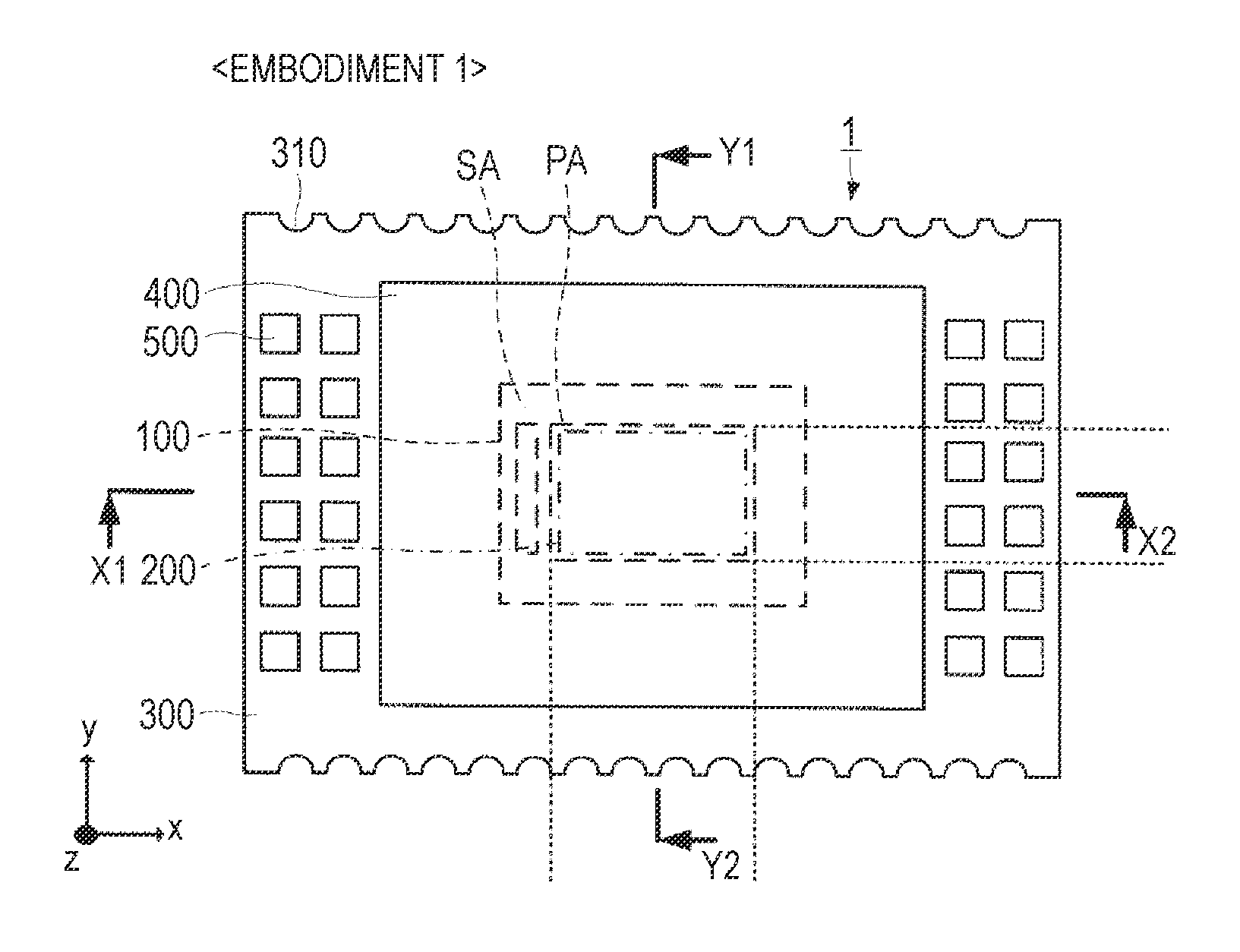
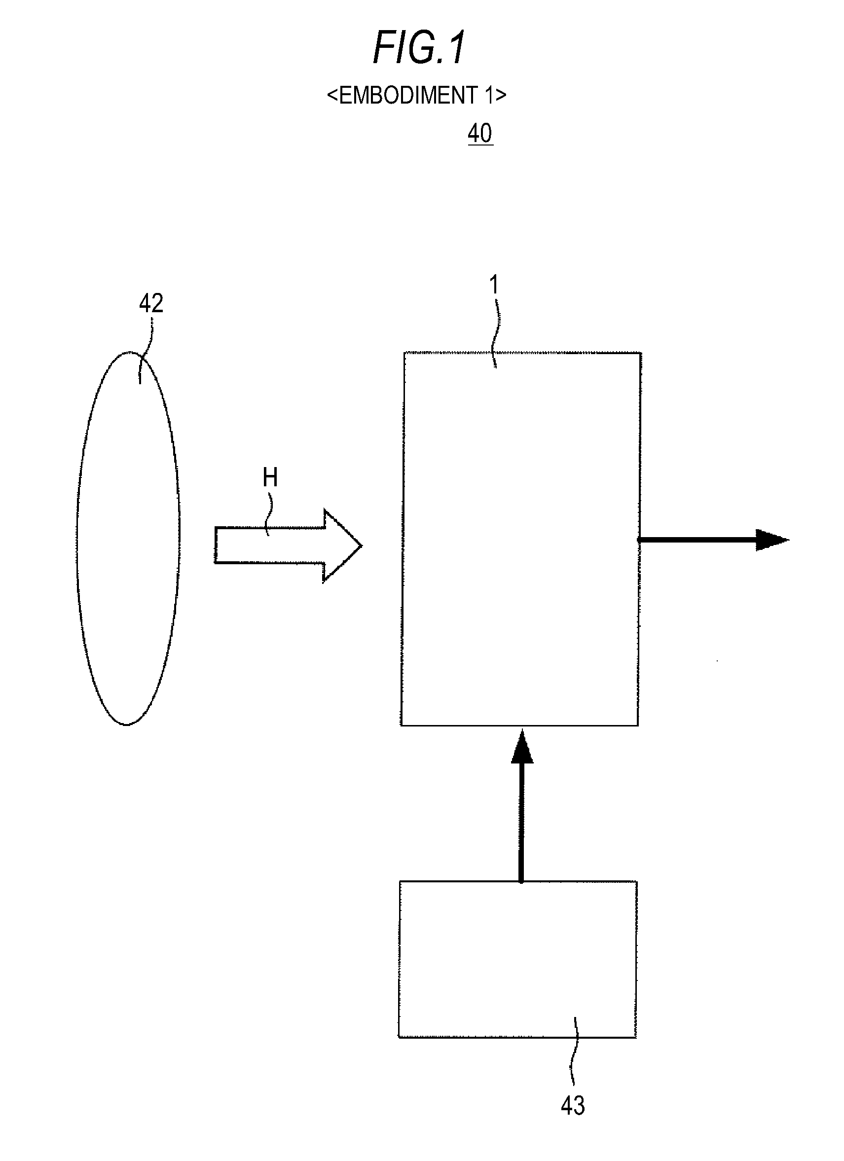
[0073]FIG. 1 is a configuration diagram showing the configuration of a camera 40 according to Embodiment 1.
[0074]As shown in FIG. 1, the camera 40 has a solid-state imaging device 1, an optical system 42, and a control section 43. The respective sections will be described in sequence.
[0075]The solid-state imaging device 1 receives incident light H input through the optical system 42 on an imaging surface and carries out photoelectric conversion to generate signal charges. Thereafter, signal processing is performed to generate and output a digital signal.
[0076]The optical system 42 includes an optical member, such as an imaging lens and / or a diaphragm, and is arranged so as to focus incident light by a subject image on the imaging surface of the solid-state imaging device 1.
[0077]The control section 43 outputs various control signals to the solid-state imaging device 1, and controls and drives the solid-...
embodiment 2
2. Embodiment 2
[A] Device Configuration and the Like
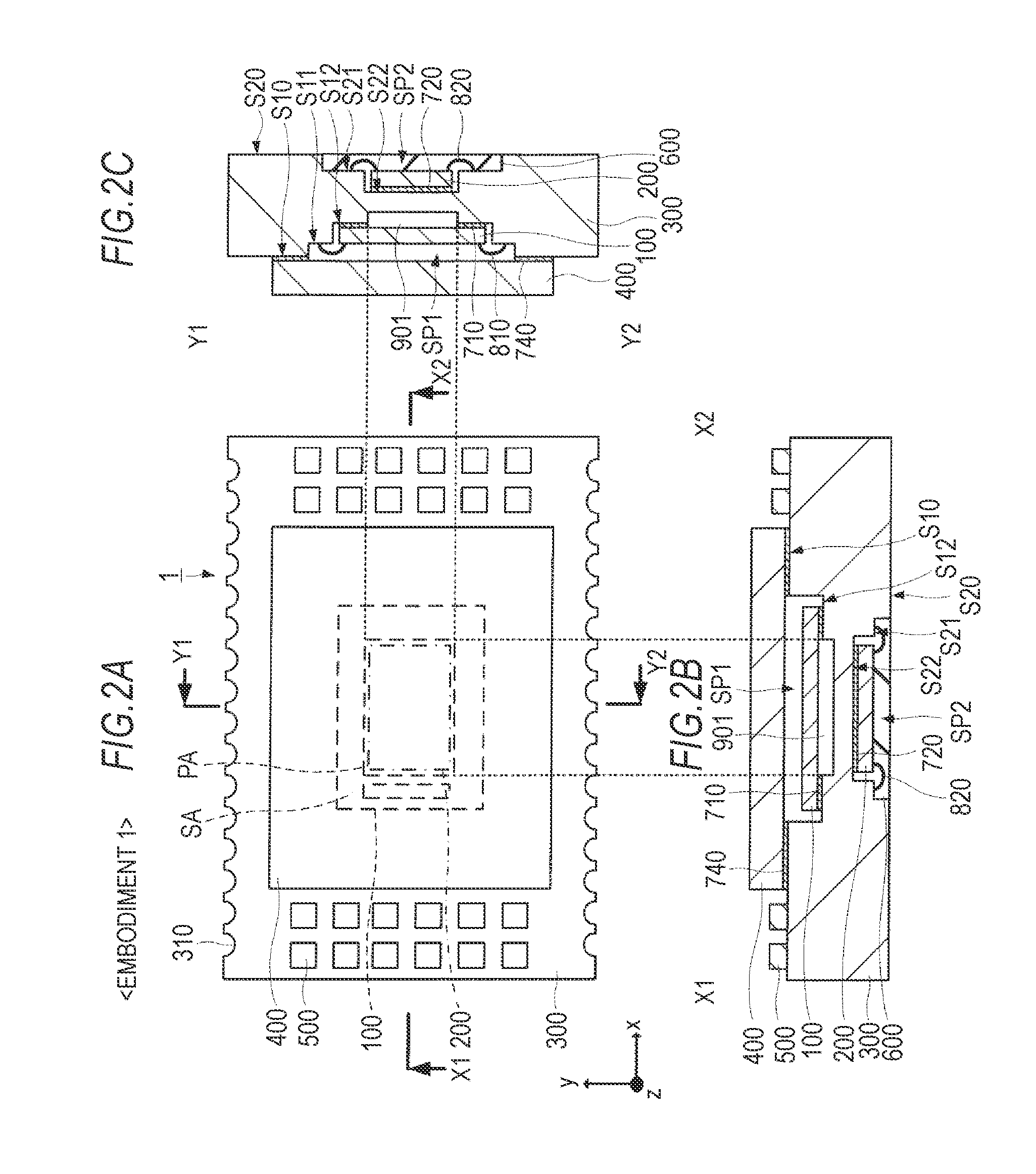
[0156]FIGS. 7A to 7C are diagrams showing the configuration of a solid-state imaging device according to Embodiment 2.
[0157]Similarly to FIGS. 2A to 2C, FIGS. 7A to 7C schematically show a configuration of the solid-state imaging device. FIG. 7A shows an upper surface of the solid-state imaging device in plan view. FIG. 7B shows a cross-section taken along the line X1-X2 of FIG. 7A. FIG. 7C shows a cross-section taken along the line Y1-Y2 of FIG. 7A.
[0158]As shown in FIGS. 7A to 7C, in this embodiment, a low-thermal-conductivity layer 902 is different from low-thermal conductivity layer 901 in Embodiment 1. This embodiment is the same as Embodiment 1, excluding this point and related points. For this reason, a description of overlapping portions will be omitted.
[0159]As shown in FIGS. 7B and 7C, as in Embodiment 1, the low-thermal-conductivity layer 902 is interposed between the image sensor chip 100 and the signal processing chip ...
embodiment 3
3. Embodiment 3
[A] Device Configuration and the Like
[0172]FIGS. 8A to 8C are diagrams showing the configuration of a solid-state imaging device according to Embodiment 3.
[0173]Similarly to FIGS. 2A to 2C, FIGS. 8A to 8C schematically show the configuration of the solid-state imaging device. FIG. 8A shows an upper surface of the solid-state imaging device in plan view. FIG. 8B shows a cross-section taken along the line X1-X2 of FIG. 8A. FIG. 8C shows a cross-section taken along the line Y1-Y2 of FIG. 8A.
[0174]As shown in FIGS. 8A to 8C, this embodiment is different from Embodiment 1 in that a plurality of low-thermal-conductivity layers 901 and 902 are provided. This embodiment is the same as Embodiment 1, excluding this point and related points. For this reason, description of the overlapping portions will be omitted.
[0175]In this embodiment, as shown in FIGS. 8B and 8C, as in Embodiment 1, a low-thermal-conductivity layer 901 is provided in the upper surface of the multilayer wirin...
PUM
 Abstract
Description
Claims
Application Information