

Electrophoretic display device and method of fabrication thereof
- Summary
- Abstract
- Description
- Claims
- Application Information
AI Technical Summary
Benefits of technology
Problems solved by technology
Method used
Image

Examples
first embodiment
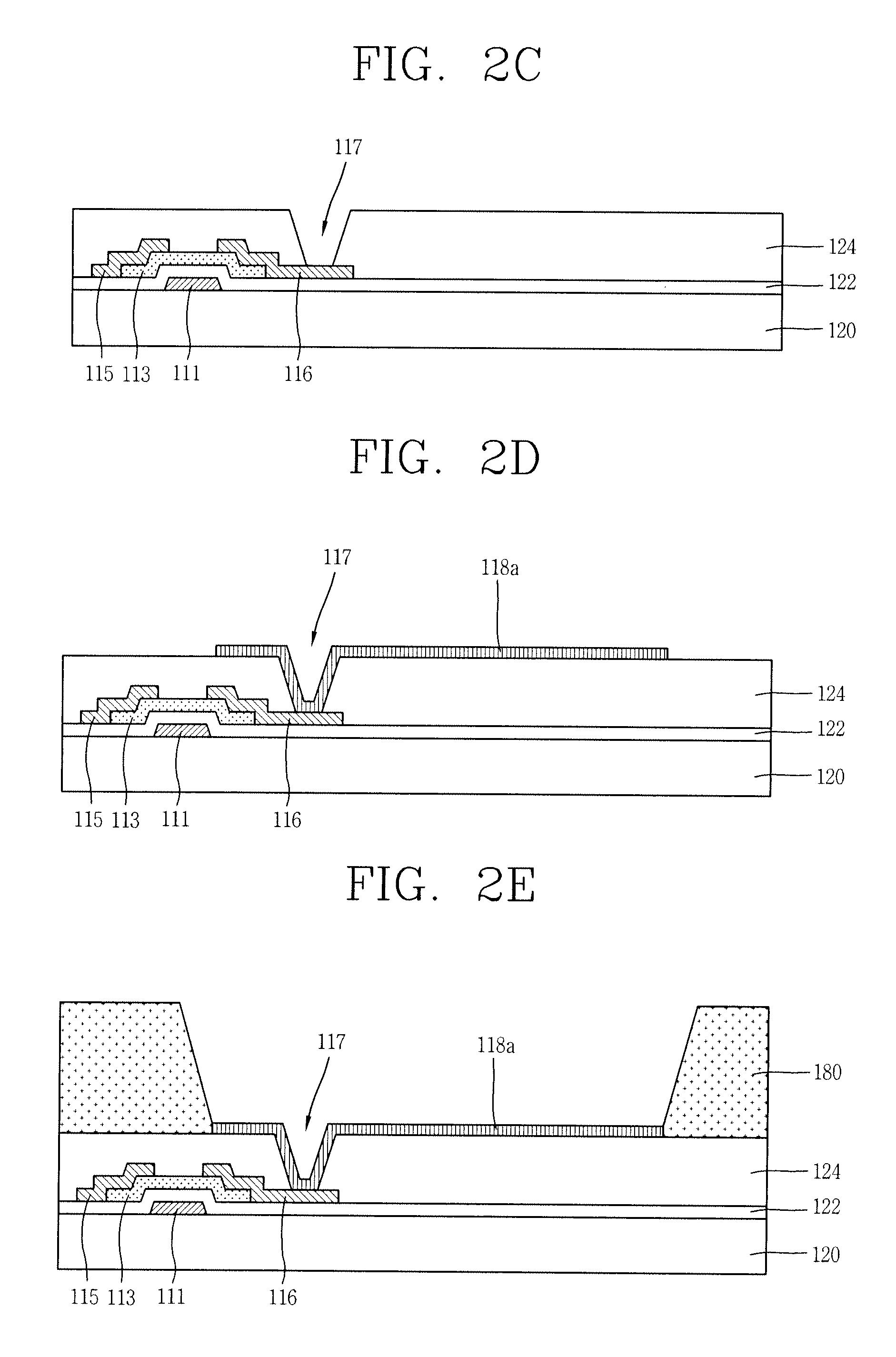
[0037]FIGS. 2A through 2H are sectional views illustrating a method of fabricating an electrophoretic display device according to the present invention. Generally, an electrophoretic display (EPD) device is comprised of a plurality of unit pixels, but for the sake of convenience of explanation, only one pixel is illustrated in the drawings.
[0038]The terms used in this embodiment will be defined. A display region refers to a region where pixels are arranged on the first substrate, and a non-display region refers to an outer portion of the display region, namely, a region where pixels are not formed thereon.
[0039]First, as illustrated in FIG. 2A, a non-transparent metal such as Cr, Mo, Ta, Cu, Ti, Al or Al alloy, having a good conductivity is deposited on a first substrate 120 comprised of a display region and a non-display region and formed of a transparent material such as glass, plastic or the like, using a sputtering process. The non-transparent material is then etched by a photol...
second embodiment
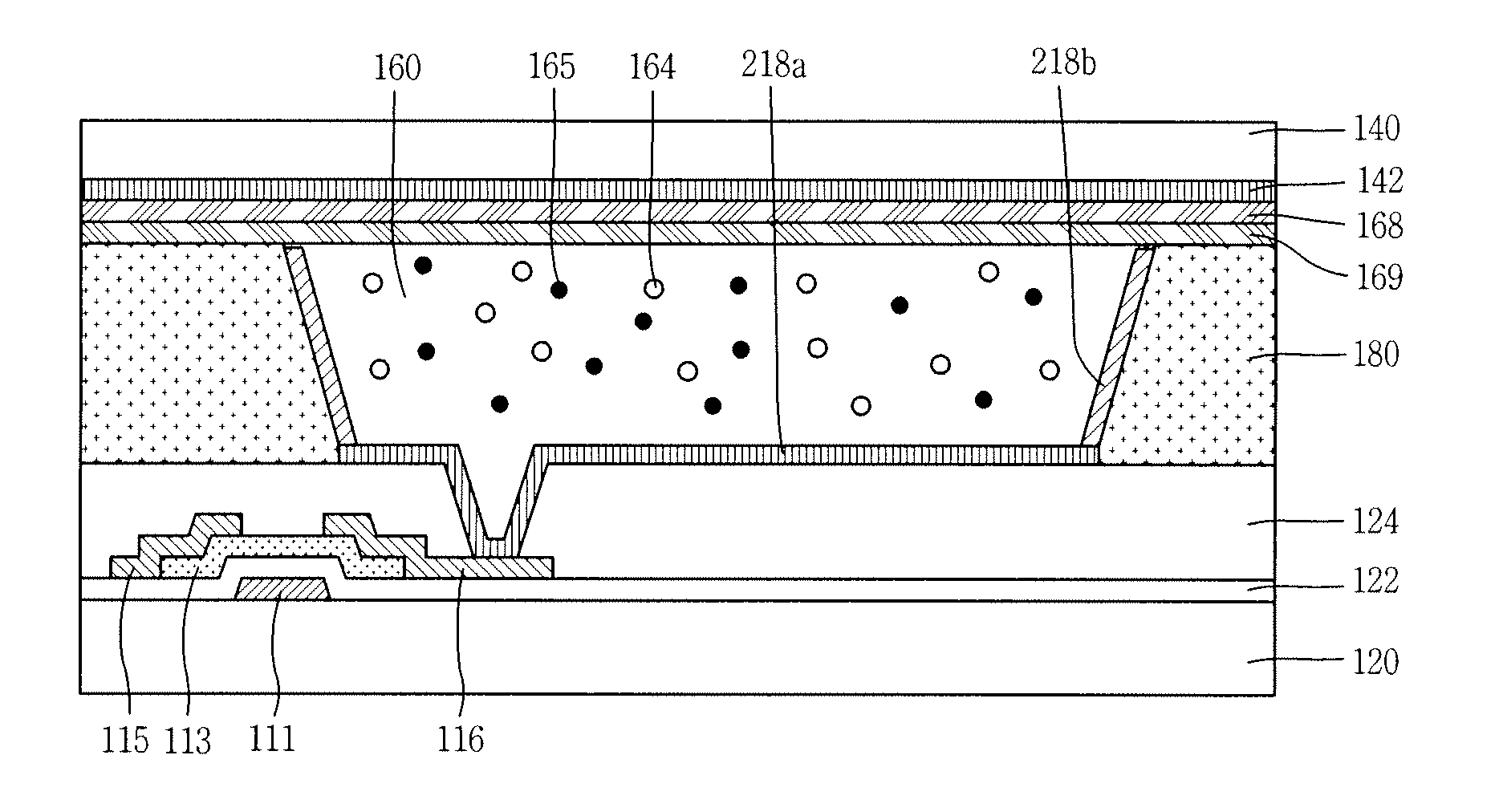
[0094]FIG. 4 is a sectional view illustrating the structure of an electrophoretic display device according to the present invention. As illustrated in FIG. 4, an electrophoretic display device according to this embodiment has the same structure except for the shape of the pixel electrode 218, compared to the electrophoretic display device illustrated in FIG. 2H. Accordingly, only the structure different therefrom will be primarily described in the following description.
[0095]As illustrated in FIG. 4, the first pixel electrode 218a is formed on the passivation layer 124 and the second pixel electrode 218b is formed only on a side wall of the partition wall 180. In this embodiment, the second pixel electrode 218b is formed on an end portion of first pixel electrode 218a and formed on the partition wall 180, whereas the second pixel electrode is formed on the first pixel electrode to be extended up to a side wall of the partition wall in the structure illustrated in FIG. 2H. However, e...
fourth embodiment
[0105]However, the passivation layer and partition wall may be formed in the same process. Hereinafter, the method of fabricating the electrophoretic display device according to the present invention where the passivation layer and partition wall are formed using the same process will be described with reference to FIGS. 6A through 6D.
[0106]First, as illustrated in FIG. 6A, a thin-film transistor having a gate electrode 111, a gate insulation layer 122, a semiconductor layer 113, a source electrode 115, and a drain electrode 116 is formed in a unit pixel of a first substrate 120. The thin-film transistor may be fabricated using a process similar to the process in the first embodiment illustrated in FIGS. 2A and 2B.
[0107]Subsequently, an insulation layer 424a is formed over the first substrate 120 to cover the thin-film transistor. The insulation layer 424a may be formed with a photosensitive resin.
[0108]Thereafter, as illustrated in FIG. 6B, a mask 470 is positioned above the insula...
PUM
 Abstract
Description
Claims
Application Information