

Sodium Sputtering Doping Method for Large Scale CIGS Based Thin Film Photovoltaic Materials
- Summary
- Abstract
- Description
- Claims
- Application Information
AI Technical Summary
Benefits of technology
Problems solved by technology
Method used
Image

Examples
Embodiment Construction
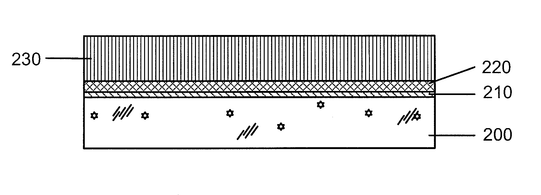
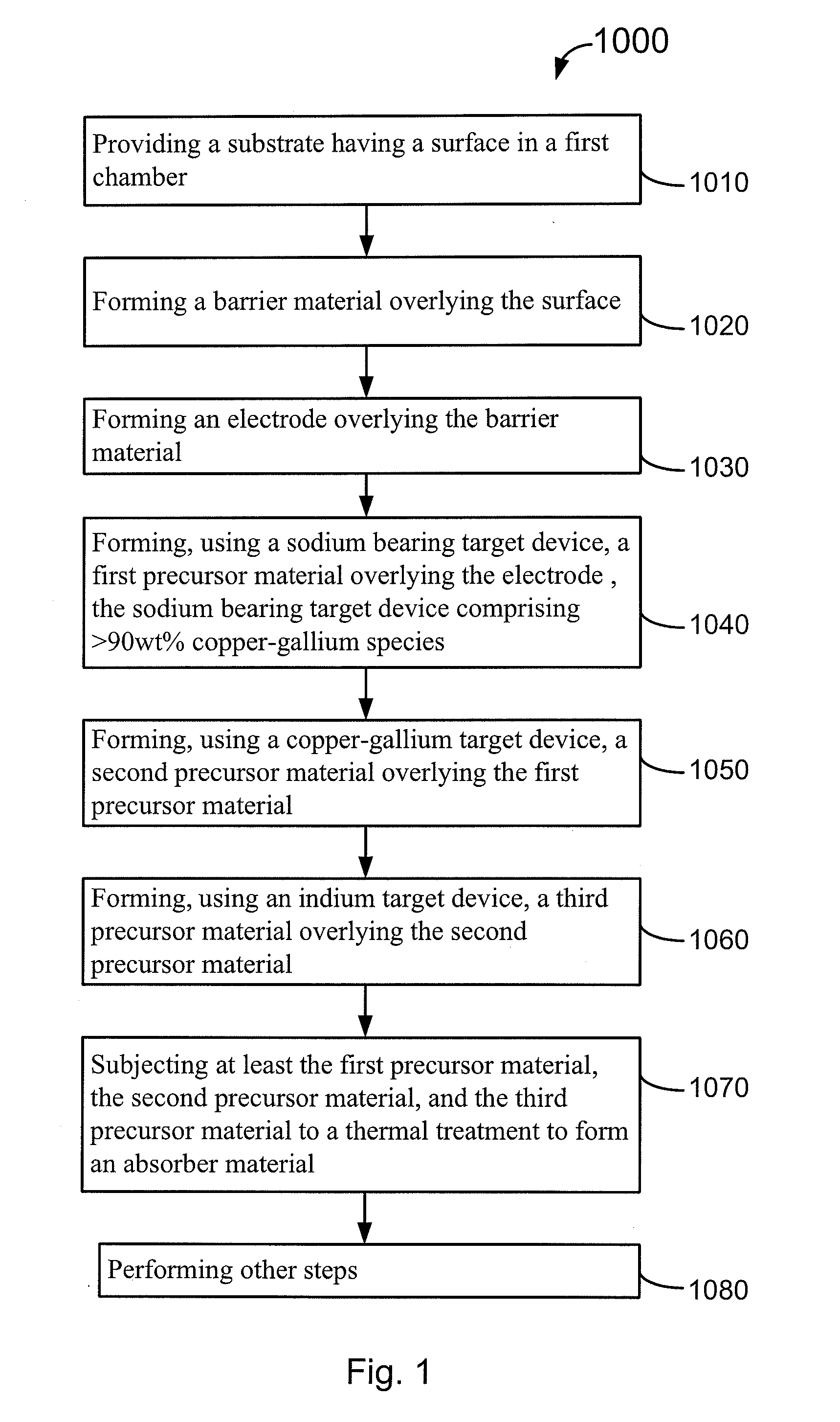
[0013]FIG. 1 is a flowchart illustrating a method of fabricating a thin-film photovoltaic material according to an embodiment of the present invention. The method 1000 includes the following processes:
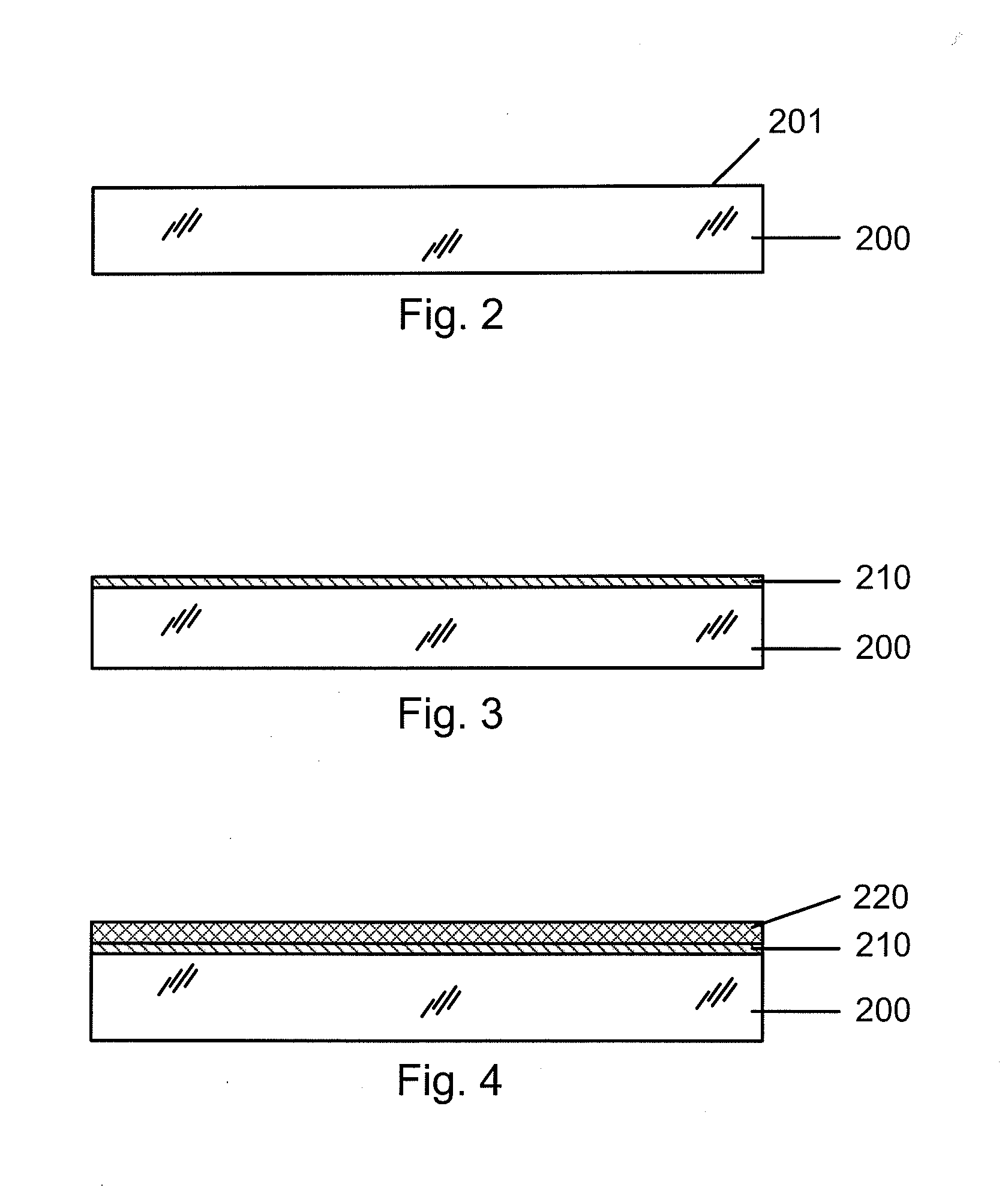
[0014]1. Process 1010 for providing a transparent substrate having a surface;
[0015]2. Process 1020 for forming a barrier material on the surface;
[0016]3. Process 1030 for forming an electrode;
[0017]4. Process 1040 for forming, using a sodium bearing target device, a first precursor material overlying the electrode, the sodium bearing target device comprising >90% copper-gallium species;
[0018]5. Process 1050 for forming, using a copper-gallium target device, a second precursor material overlying the first precursor material;
[0019]6. Process 1060 for forming, using an indium target device, a third precursor material overlying the second precursor material;
[0020]7. Process 1070 for subjecting at least the first precursor material, the second precursor material, and the third precursor mat...
PUM
 Abstract
Description
Claims
Application Information