Organic light emitting display device

a light-emitting display and organic technology, applied in the field of organic light-emitting display devices, can solve the problems of six transistors in the pixel b>4/b>, the inability to display an image with uniform luminance, and the inability to simplify the pixel b>4/b>, so as to reduce the number of transistors.

Active Publication Date: 2012-01-26
SAMSUNG DISPLAY CO LTD
View PDF3 Cites 27 Cited by
  • Summary
  • Abstract
  • Description
  • Claims
  • Application Information

AI Technical Summary

Benefits of technology

[0016]Aspects of embodiments according to the present invention are directed toward an organic light emitting display device having a simple structure and being capable of compensating for the threshold voltage of a driving transistor.
[0020]According to the pixel and the organic light emitting display device of the present invention using the same, the threshold voltage of the driving transistor could be compensated for while minimizing or reducing the number of the transistors included in the pixels.

Problems solved by technology

However, the pixel 4 of the organic light emitting display device of the related art cannot display an image with uniform luminance.
However, the six transistors in the pixel 4 complicate the pixel 4.

Method used


Image

  • Organic light emitting display device
  • Organic light emitting display device
  • Organic light emitting display device

Examples


first embodiment

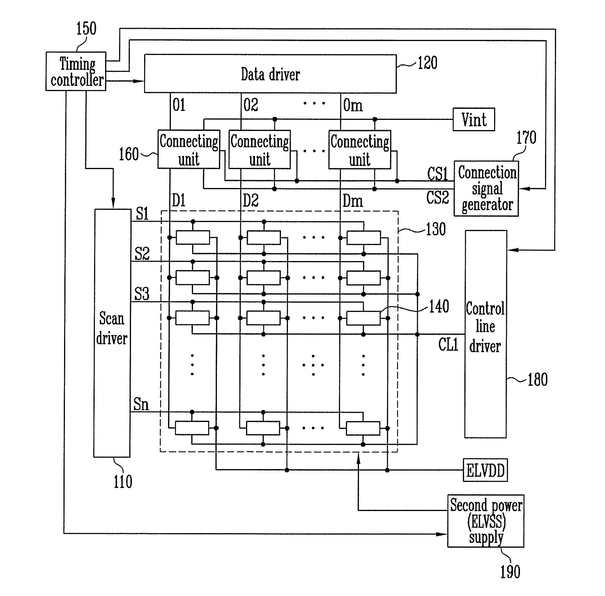
[0044]FIG. 3 is a circuit diagram showing the connecting unit 160 and the pixel 140 according to the present invention. In FIG. 3, for the convenience of description, the connecting unit 160 coupled to the m-th output line Om and the pixel 140 coupled to the n-th scan line Sn are shown.

[0045]Referring to FIG. 3, the connecting unit 160 according to the first embodiment of the present invention includes a first control transistor CM1 and a second control transistor CM2.

[0046]The first control transistor CM1 is formed between the output line Om and the data line Dm. The first control transistor CM1 is turned on when the first connecting signal CS1 is supplied.

[0047]The second control transistor CM2 is formed between the data line Dm and the initial power supply Vint. The second control transistor CM2 is turned on when the second connecting signal CS2 is supplied.

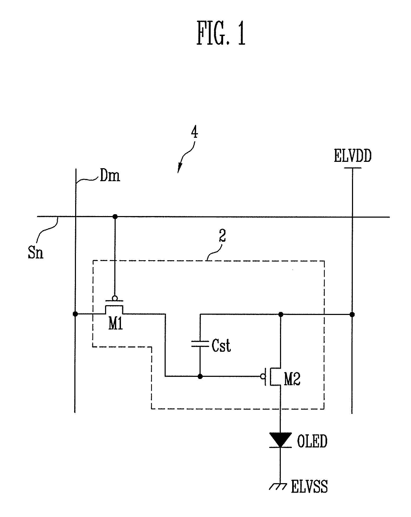
[0048]The pixel 140 according to an embodiment of the present invention includes the organic light emitting diode OLED and a...

second embodiment

[0070]FIG. 5 is a circuit diagram showing a connecting unit 160 and a pixel 140 according to the present invention. For convenience, when describing FIG. 5, the same components as described in FIG. 3 are referred to by the same reference numerals, and their detail descriptions will not be provided.

[0071]Referring to FIG. 5, the pixel 140 according to the second embodiment of the present invention includes an organic light emitting diode OLED and a pixel circuit 142′ that controls the amount of current supplied to the organic light emitting diode OLED.

[0072]An anode electrode of the organic light emitting diode OLED is coupled to the pixel circuit 142′, and a cathode electrode is coupled to the second power supply ELVSS. The organic light emitting diode OLED generates light having predetermined luminance corresponding to the current supplied from the pixel circuit 142′.

[0073]The pixel circuit 142′ is charged at a voltage corresponding to the threshold voltage of the driving transisto...

third embodiment

[0083]FIG. 7 is a circuit diagram showing a connecting unit 160 and a pixel 140 according to the present invention. For convenience, when describing FIG. 7, the same components as described in FIG. 3 are referred to by the same reference numerals, and their detail descriptions will not be provided.

[0084]Referring to FIG. 7, the pixel 140 according to the third embodiment of the present invention includes the organic light emitting diode OLED and a pixel 142″ for controlling the amount of current supplied to the organic light emitting diode OLED.

[0085]The anode electrode of the organic light emitting diode OLED is coupled to the pixel circuit 142″, and the cathode electrode is coupled to the second power supply ELVSS. The organic light emitting diode OLED generates light having predetermined luminance corresponding to the current supplied from the pixel circuit 142″.

[0086]The pixel circuit 142″ is charged at a voltage corresponding to the threshold voltage of the driving transistor a...


PUM


Abstract

An organic light emitting display device operates for an initializing period, a scan period and an emission period divided from one frame period. The organic light emitting display device includes: a data driver for supplying data signals to output lines; a connecting unit for selectively coupling a data line of data lines to a corresponding one of the output lines or an initial power supply, and being positioned between the output lines and the data lines; a second power driver for applying second power having a low level and a high level to pixels positioned at crossing regions of scan lines and the data lines; and a first control line commonly coupled to the pixels, in which each of the pixels includes an organic light emitting diode, and an anode electrode of the organic light emitting diode is supplied with a voltage of the initial power supply for the initializing period.

Description

CROSS-REFERENCE TO RELATED APPLICATION[0001]This application claims priority to and the benefit of Korean Patent Application No. 10-2010-0069938, filed on Jul. 20, 2010, in the Korean Intellectual Property Office, the entire content of which is incorporated herein by reference.BACKGROUND[0002]1. Field[0003]Aspects of embodiments according to the present invention relate to an organic light emitting display device.[0004]2. Description of the Related Art[0005]Recently, flat panel display devices having reduced weight and volume in comparison to a cathode ray tube are being developed. The flat panel display devices include liquid crystal displays, field emission displays, plasma display panels and organic light emitting display devices, and the like.[0006]The organic light emitting display device displays an image using organic light emitting diodes that produce light by recombining electrons and holes. The organic light emitting display device has the advantage that it has fast respon...

Claims


Application Information

Patent Timeline
Patent Type & Authority Applications(United States)
IPC IPC(8): G09G5/00G09G3/30
CPCG09G3/325G09G2300/0861G09G2320/045G09G2310/0262G09G2320/0233G09G2310/0251
Inventor HWANG, YOUNG-INPARK, YONG-SUNGKANG, CHUL-KYUPARK, SEONG-IL
Owner SAMSUNG DISPLAY CO LTD
Why Eureka
Try Eureka