Intergrated pump laser and rare earth waveguide amplifier

a rare earth oxide and laser technology, applied in lasers, fiber transmission, transmission, etc., can solve the problems of inefficient operation, difficult incorporating electronics for controlling, monitoring, etc., and reducing the overall footprint of light amplifiers, so as to improve fabricating techniques and interconnections.

Inactive Publication Date: 2012-01-26
IQE
View PDF2 Cites 9 Cited by
  • Summary
  • Abstract
  • Description
  • Claims
  • Application Information

AI Technical Summary

Benefits of technology

[0013]By integrating the light amplifier, other electronic components, such as control and/or monitoring apparatus, can be integrated with the light amplifier to greatl

Problems solved by technology

A major problem with the prior art EDWA is that the pump laser is bonded to the Erbium doped waveguide by either wafer bonding or by bump bonding.
In either bonding method, the footprint of the final product

Method used


Image

  • Intergrated pump laser and rare earth waveguide amplifier
  • Intergrated pump laser and rare earth waveguide amplifier
  • Intergrated pump laser and rare earth waveguide amplifier

Examples


Embodiment Construction

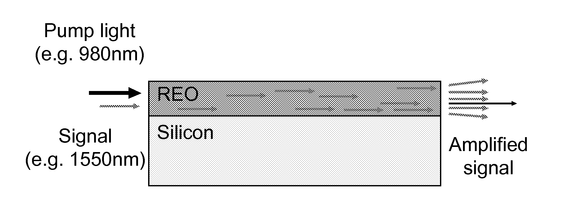
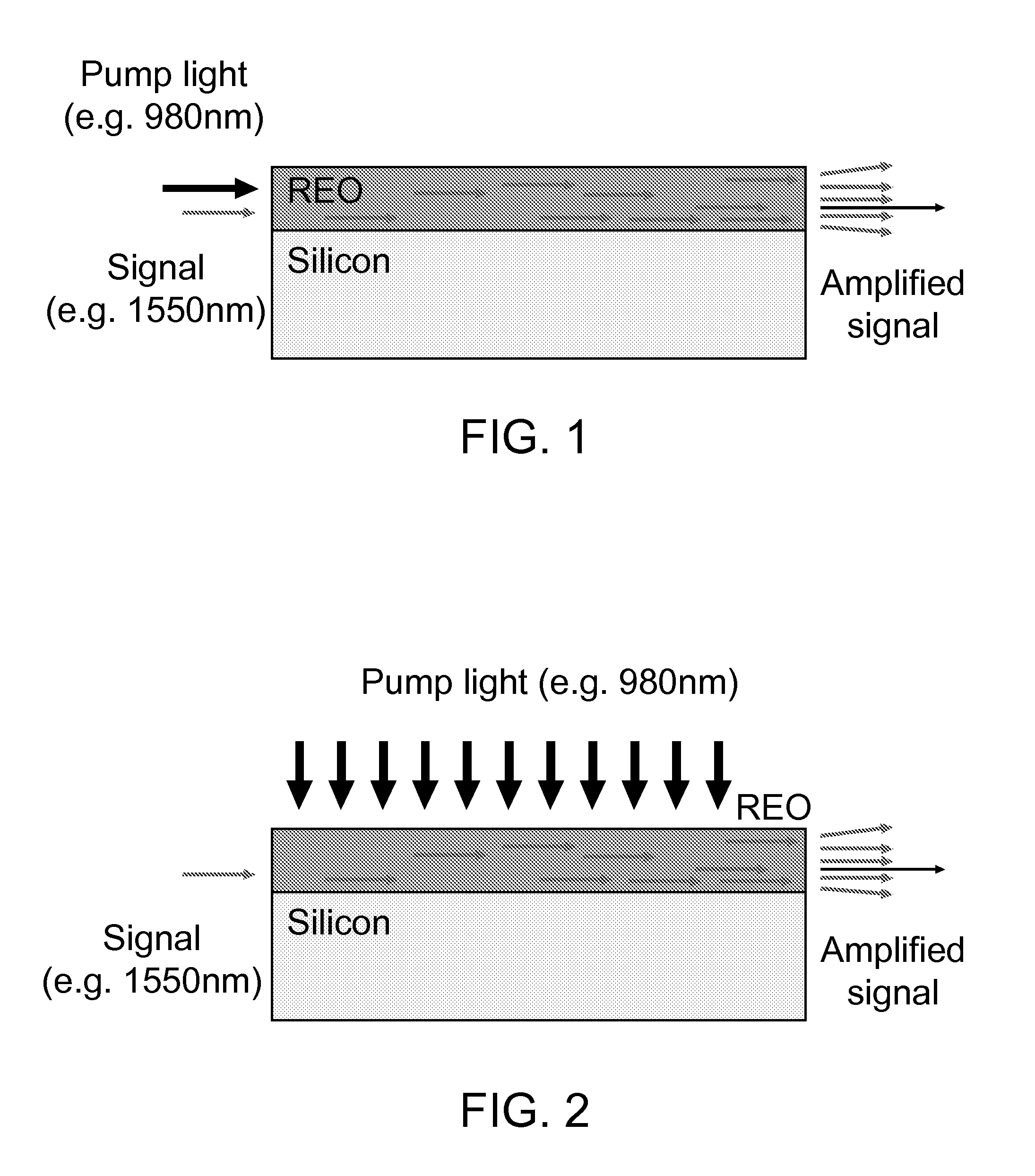
[0023]Turning now to the drawings, attention is first directed to FIGS. 1 and 2, which illustrate prior art longitudinally and vertically pumped Erbium Doped Waveguide Amplifiers (EDWAs), respectively. In each of these applications the pump laser, not shown, is attached to the EDWA by bump bonding or wafer bonding. As understood by artisans, the pump laser is fabricated on a separate substrate with individual or discrete pump lasers bonded to an EDWA in a separate and relatively complicated process.

[0024]The wafer bonding process involves fabricating the pump laser on the surface of a separate substrate. The pump laser output surface is then brought into contact with the surface of the EDWA and forms a molecular bond through a well known process, referred to in the industry as Van der Waal's bonding. The substrate carrying the pump laser is then partially removed by any of several different methods to reduce the overall bulk of the final product. The entire process is very labor int...


PUM


Abstract

A light amplifier includes a single crystal semiconductor substrate with a rare earth oxide, light amplifying gain medium deposited on the substrate and formed into a light waveguide, and a pump laser. A lattice matching virtual substrate integrates the pump laser to the gain medium with a first opposed surface crystal lattice matched to the gain medium and second opposed surface crystal lattice matched to the pump laser. The pump laser is positioned with a light output surface coupled to a light input surface of the gain medium so as to introduce pump energy into the light waveguide. The light amplifier has a very small footprint and allows the integration of control and monitoring electronics.

Description

FIELD OF THE INVENTION[0001]This invention relates to light amplifiers and more particularly, to the integration of pump lasers with rare earth oxide doped waveguide amplifiers to reduce the footprint.BACKGROUND OF THE INVENTION[0002]Erbium doped waveguide lasers are known in the art. Basically, a pump laser injects (pumps) 980 nm light into an Erbium doped waveguide carrying a light signal at for example 1550 nm. The Erbium doped waveguide substantially absorbs the 980 nm light and converts it to 1550 nm or amplifies the light signal. Thus, the Erbium doped waveguide is an amplifier of the light signal, i.e. an Erbium doped waveguide amplifier (EDWA).[0003]A major problem with the prior art EDWA is that the pump laser is bonded to the Erbium doped waveguide by either wafer bonding or by bump bonding. In either bonding method, the footprint of the final product and the amount of labor and process steps required are greatly increased. Also, incorporating electronics for controlling, ...

Claims


Application Information

Patent Timeline
IPC IPC(8): H01S3/00H01L21/30
CPCH01S3/0632H01S3/0635H01S3/0637H01S3/0941H01S3/09415H01S5/42H01S5/0207H01S5/0218H01S5/026H01S5/183H01S5/32341H01S3/1603
Inventor WILLIAMS, DAVID L.CLARK, ANDREWLEBBY, MICHAEL
Owner IQE
Why Eureka
Try Eureka