

Ceramic electronic component
- Summary
- Abstract
- Description
- Claims
- Application Information
AI Technical Summary
Benefits of technology
Problems solved by technology
Method used
Image

Examples
first preferred embodiment
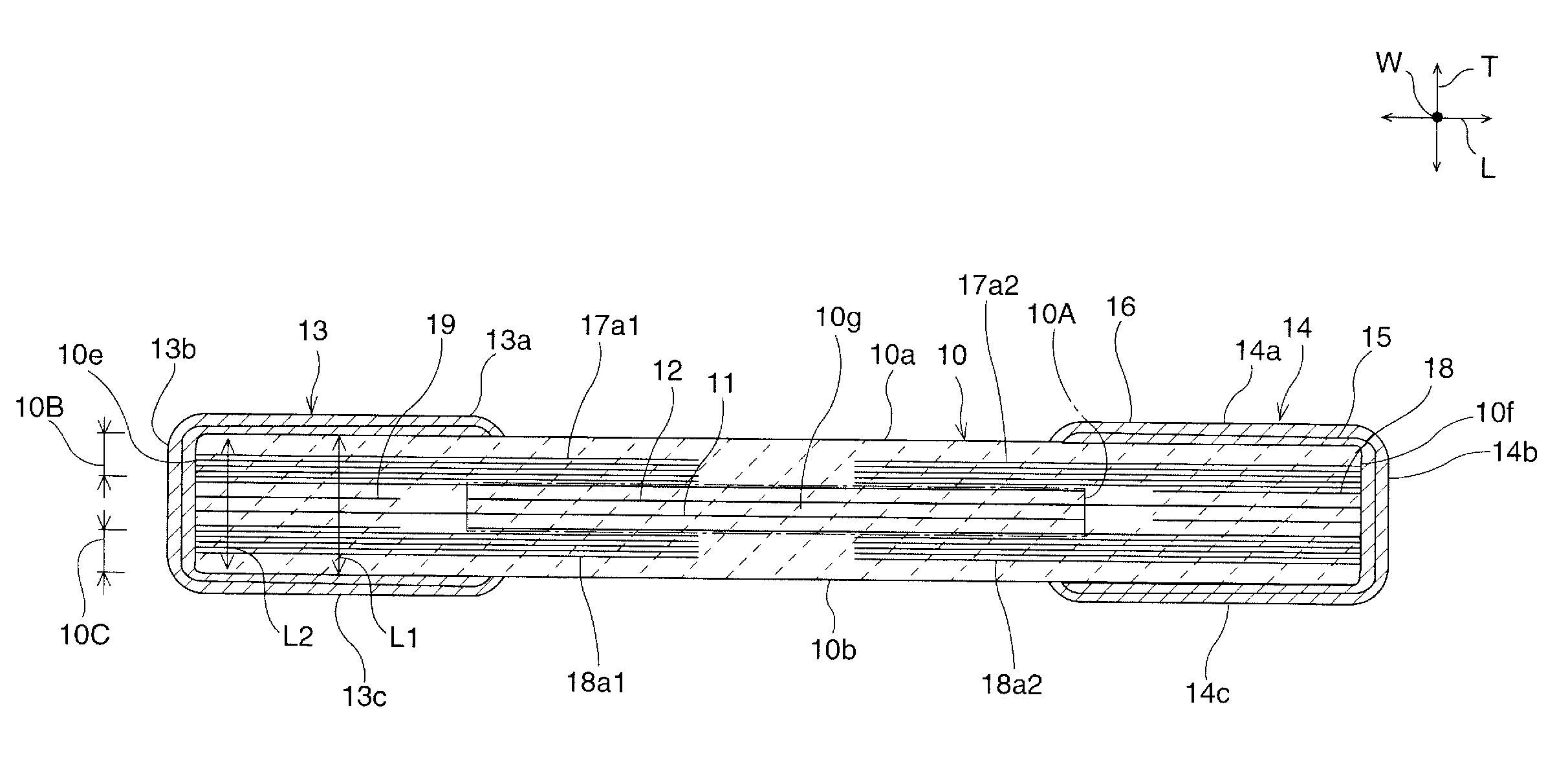
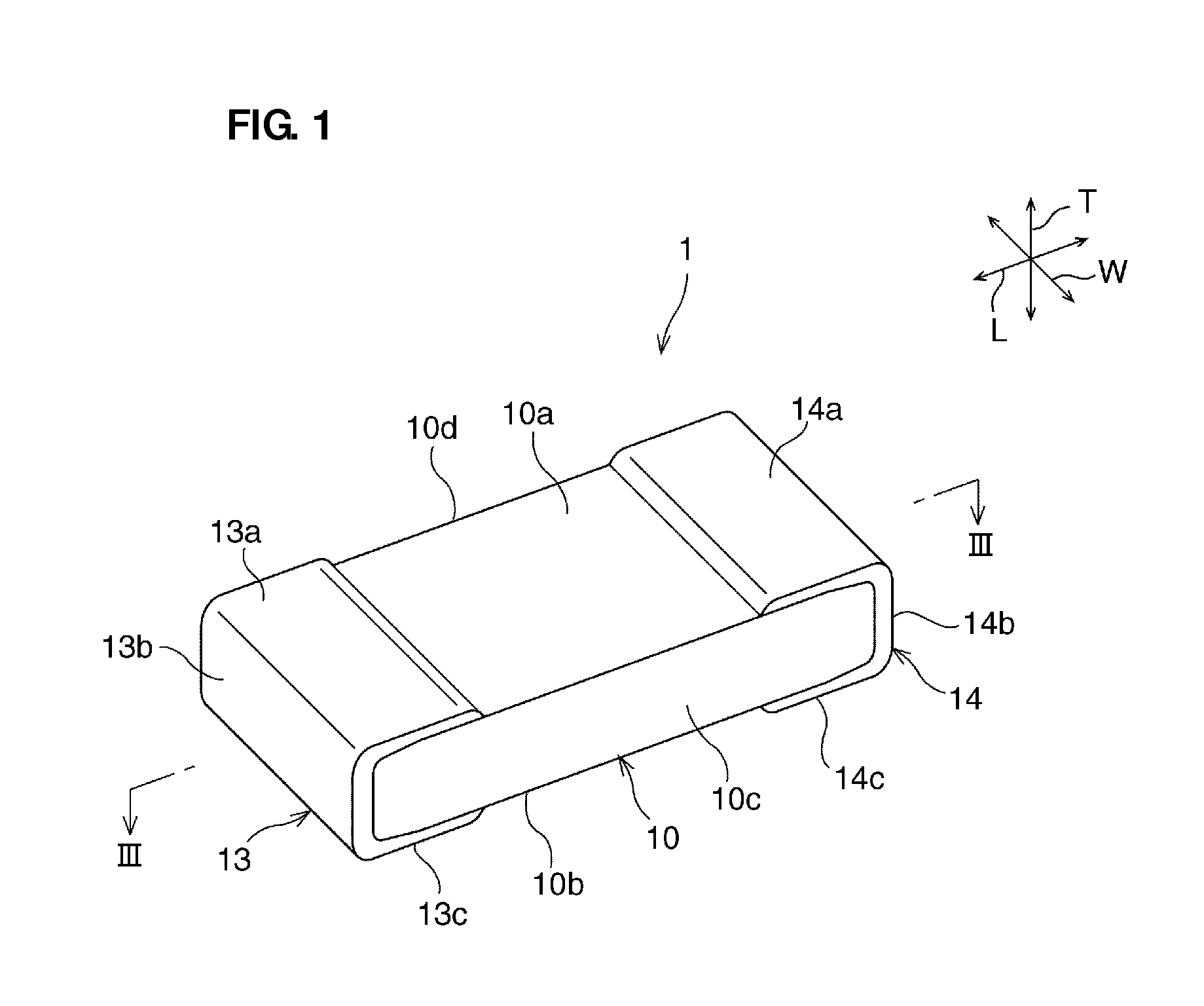
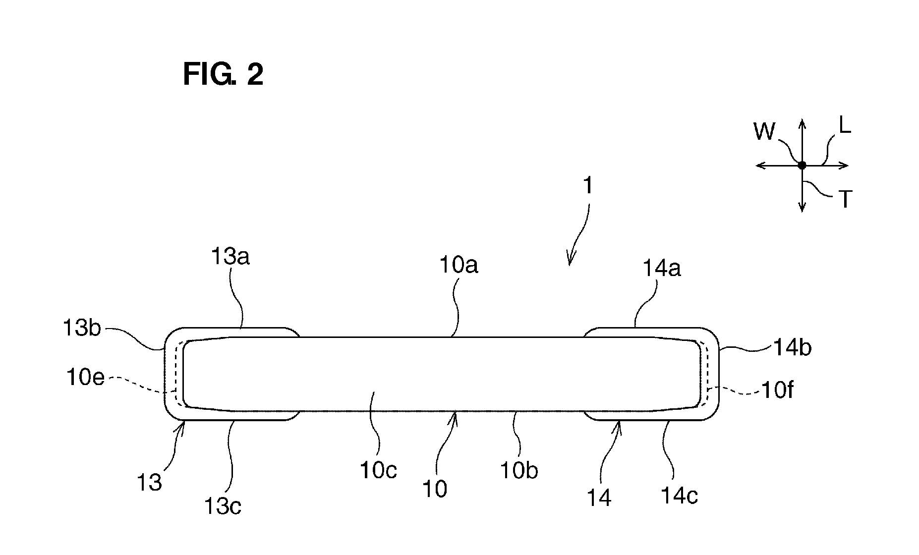
[0032]A first preferred embodiment of the present invention will be described hereinafter in the context of a ceramic electronic component 1 illustrated in FIG. 1, by way of example. However, the ceramic electronic component 1 is merely illustrative. Preferred embodiments of the present invention are not limited to the ceramic electronic component 1 described below and a method for manufacturing the ceramic electronic component 1.
[0033]FIG. 1 is a schematic perspective view of a ceramic electronic component according to the first preferred embodiment of the present invention. FIG. 2 is a schematic side view of the ceramic electronic component according to the first preferred embodiment. FIG. 3 is a schematic cross-sectional view taken along line III-III in FIG. 1. FIG. 4 is a schematic cross-sectional view of an enlarged portion of the ceramic electronic component according to this preferred embodiment. FIG. 5 is a schematic cross-sectional view taken along line V-V in FIG. 3.
[0034]...
second preferred embodiment
[0104]FIG. 13 is a schematic cross-sectional view of a ceramic electronic component according to a second preferred embodiment of the present invention.
[0105]In this preferred embodiment, as illustrated in FIG. 13, at least a portion of the first and third portions 13a and 14a and 13c and 14c of the first and second external electrodes 13 and 14 is preferably embedded in the first main surface 10a or the second main surface 10b. Even in this case, similarly to the first preferred embodiment, the mechanical durability of the ceramic electronic component 1 is effectively improved.
[0106]The ceramic electronic component according to this preferred embodiment may be formed by, for example, printing, on the main surfaces of a mother laminate 22, conductor patterns 23 having shapes corresponding to the portions defining the first and third portion 13a and 14a and 13c and 14c and then by pressing the mother laminate in the stacking direction such that the mother laminate 22 is pressed with ...
third preferred embodiment
[0107]FIG. 14 is a schematic cross-sectional view of a ceramic electronic component according to a third preferred embodiment of the present invention.
[0108]In the first preferred embodiment, the first and second external electrodes 13 and 14 are preferably provided on each of the first and second main surfaces 10a and 10b, by way of example. However, the present invention is not limited to this configuration, and at least one external electrode may be provided on the first main surface 10a.
[0109]For example, as illustrated in FIG. 14, the first and second external electrodes 13 and 14 may preferably be arranged so as to cover the first end surface 10e or the second end surface 10f and the first main surface 10a. That is, as long as the first and second external electrodes 13 and 14 include the first portions 13a and 14a, respectively, and are electrically connected to the first internal electrode 11 or the second internal electrode 12, the shapes of the first and second external e...
PUM
| Property | Measurement | Unit |
|---|---|---|
| Thickness | aaaaa | aaaaa |
| Length | aaaaa | aaaaa |
Abstract
Description
Claims
Application Information