Reference current source circuit including added bias voltage generator circuit

a current source circuit and reference current technology, applied in the direction of electric variable regulation, process and machine control, instruments, etc., can solve the problems of increasing circuit area and power consumption, increasing current amount, sensitive variation of characteristics, etc., and achieve the effect of reducing the circuit area

Inactive Publication Date: 2012-02-02
SEMICON TECH ACADEMIC RES CENT
View PDF13 Cites 35 Cited by
  • Summary
  • Abstract
  • Description
  • Claims
  • Application Information

AI Technical Summary

Benefits of technology

[0019]It is an object of the present invention to provide a reference current source circuit capable of solving the above-described problems, reducing the circuit area as compared with that of the prior art, and controlling an inclination of a temperature characteristic of an output current to be zero at a room temperature.
[0029]According to the reference current source circuit of the present invention, the added bias generator circuit generates the added bias voltage, which has the predetermined temperature coefficient and includes the predetermined offset voltage, and the drain bias voltage generator circuit adds the added bias voltage to the drain bias voltage and applies the voltage of the adding results to the drain of the MOS resistor. Therefore, the inclination of the temperature characteristic of the output current can be controlled to be zero at the room temperature, and the reference current source circuit can supply a constant output current stable to variations (referred to as PVT variations hereinafter) including a process variation, a power supply voltage variation and a temperature variation. In addition, since the added bias generator circuit has one current path, the reference current source circuit of the present invention can be configured to have a circuit area equal to or smaller than half of that of the prior art current source circuit, and the power consumption can be reduced.
[0030]In addition, according to the reference current source circuit of the present invention, by using only one common nMOS transistor instead of the first nMOS transistor that operates in the subthreshold saturation region in the added bias generator circuit and the nMOS transistor that operates in the subthreshold saturation region in the drain bias voltage generator circuit, the number of transistors can be reduced as compared with that of the above-described reference current source circuit.

Problems solved by technology

Electrical characteristics of a MOSFET in the subthreshold region have such a problem that the characteristics sensitively vary with respect to temperature changes and process variations.
However, when the voltage source circuit is used as a current source, a current flowing through the voltage source circuit has a temperature characteristic, and this has led such a problem that the amount of current increases when the temperature rises.
However, this current source circuit requires using two current source circuits that have complementary structures for generating the currents dependent on the mobilities of two kinds, and requires using a current subtracting circuit for the subtraction of the currents, and this leads to such a problem that the circuit area and the power consumption increase.

Method used


Image

  • Reference current source circuit including added bias voltage generator circuit
  • Reference current source circuit including added bias voltage generator circuit
  • Reference current source circuit including added bias voltage generator circuit

Examples


first preferred embodiment

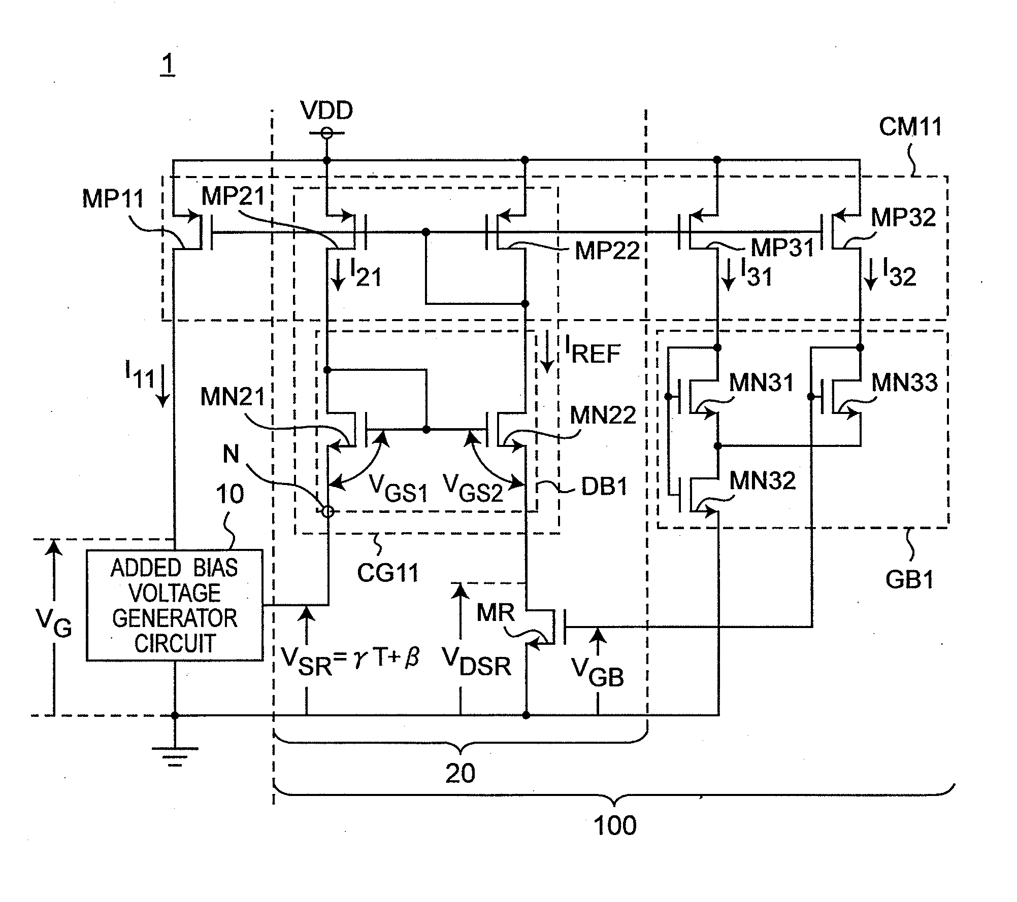
[0049]A reference current source circuit 1 according to the first preferred embodiment of the present invention is configured to further include an added bias generator circuit 10 for generating an added bias voltage VSR including a minute offset voltage β in the voltage source circuit disclosed in the Non-Patent Document 1, so as to improve the temperature dependence of an output current IREF.

[0050]FIG. 1 is a circuit diagram showing a configuration of the reference current source circuit 1 according to the first preferred embodiment of the present invention. Referring to FIG. 1, the reference current source circuit 1 is configured to include a current source circuit 100 and the added bias generator circuit 10. Further, the current source circuit is configured to include a current mirror circuit CM11, a gate bias voltage generator circuit GB1, a drain bias voltage generator circuit DB1, and a MOS resistor MR.

[0051]The reference current source circuit 1 of the first preferred embodi...

second preferred embodiment

[0082]FIG. 7 is a circuit diagram showing a configuration of a reference current source circuit 1A according to the second preferred embodiment of the present invention. The reference current source circuit 1A is characterized in that a startup circuit 40 is further provided as compared with the reference current source circuit 1 of FIG. 1. The other components are similar to those of the reference current source circuit 1, and therefore, no description is provided for them.

[0083]The reason why the startup circuit 40 is provided is as follows. In the reference current source circuit 1, it is possibly a case where all of the gate voltages of the nMOS transistors are 0 V, and all of the gates of the pMOS transistors have voltages generated by the power source VDD. In this case, no operating current flows through the reference current source circuit 1, and the reference current source circuit 1 does not operate. This state in which the reference current source circuit 1 does not operat...

third preferred embodiment

[0088]FIG. 8 is a circuit diagram showing a configuration of a reference current source circuit 1B according to the third preferred embodiment of the present invention. The reference current source circuit 1B of FIG. 8 is characterized in that an added bias generator circuit 10 is further provided with a reference current source circuit 100B disclosed in the Non-Patent Document 7. In this case, the added bias generator circuit 10 of FIG. 8 has a configuration similar to that of the added bias generator circuit 10 as described in the first preferred embodiment, and operates in a manner similar to above.

[0089]Referring to FIG. 8, the reference current source circuit 1B is configured to include the reference current source circuit 100B and the added bias generator circuit 10. Further, the reference current source circuit 100B is configured to include a MOS resistor MR, a current mirror circuit CM12 including pMOS transistors MP1, MP2, MP3, MP4 and MP5, a gate bias voltage generator cir...


PUM


Abstract

A MOS resistor generates an output current based on a voltage induced across a drain and a source thereof. A gate bias voltage generator circuit generates a gate bias voltage so as to operate the MOS resistor in a strong-inversion linear region, and applies the gate bias voltage to a gate of the MOS resistor. A drain bias voltage generator circuit generates a drain bias voltage, and applies the drain bias voltage to the drain of the MOS resistor. An added bias voltage generator circuit generates an added bias voltage, which has a predetermined temperature coefficient and includes a predetermined offset voltage, so that the output current becomes constant against temperature changes. The drain bias voltage generator circuit adds the added bias voltage to the drain bias voltage, and applies a voltage of adding results to the drain of the MOS resistor as the drain bias voltage.

Description

[0001]The disclosure of Japanese Patent Application No. 2010-172391 filed Jul. 30, 2010 including specification, drawings and claims is incorporated herein by reference in its entirety. In addition, the disclosure of Japanese Patent Application No. 2011-157568 filed Jul. 19, 2011 including specification, drawings and claims is incorporated herein by reference in its entirety.BACKGROUND OF THE INVENTION[0002]1. Field of the Invention[0003]The present invention relates to a reference current source circuit including Metal Oxide Semiconductor Field Effect Transistors operated in a subthreshold region.[0004]2. Description of the Related Art[0005]As a technique for remarkably reducing the power consumption of a circuit system, there has been a method of designing a circuit system on such an assumption that a Metal Oxide Semiconductor Field Effect Transistor (referred to as a MOSFET hereinafter) is operated in the subthreshold region. Electrical characteristics of a MOSFET in the subthres...

Claims


Application Information

Patent Timeline
Patent Type & Authority Applications(United States)
IPC IPC(8): G05F3/16
CPCG05F3/242
Inventor HIROSE, TETSUYAOSAKI, YUJI
Owner SEMICON TECH ACADEMIC RES CENT
Why Eureka
Try Eureka