Imaging device, external flash detection method, program, and integrated circuit

a flash detection and imaging device technology, applied in the field of imaging devices, can solve the problems of white band-shaped artifacts appearing in video, white band-shaped artifacts appearing in captured screens, etc., and achieve the effects of small circuit scale, increased circuit scale, and reliable determination

Active Publication Date: 2012-02-02
PANASONIC CORP
View PDF1 Cites 37 Cited by
  • Summary
  • Abstract
  • Description
  • Claims
  • Application Information

AI Technical Summary

Benefits of technology

[0177]The present invention enables achieving an imaging device, an external flash detection method, a program, and an integrated circuit that can reliably determine whether an imaging signal has been influenced by an external flash emitted at an arbitrary time without inviting an increase in the circuit scale.
[0178]The present invention also enables achieving an imaging device, an external flash detection method, a program, and an integrated circuit that can perform flash presence detection with respect to an unnatural image including a bright horizontal band due to an external flash and with respect to a moving high-luminance subject with a small circuit scale and few erroneous operations.

Problems solved by technology

A CMOS image sensor therefore has disadvantages that a CCD image sensor does not have, due to the fact that the accumulated charged readout time is shifted, and the timing of the accumulation period of each pixel is shifted.
One example of a problem is the phenomenon in which white band-shaped artifacts appear in the captured screen when a video camera with a CMOS image sensor captures images of a subject being illuminated with flashes from a still camera or the like.
In this way, with an imaging device that uses a CMOS image sensor, there is the first problem that white band-shaped artifacts appear in a video formed by an imaging signal when an external flash is emitted.
Also, with an imaging device that uses a CMOS image sensor, there is the second problem that performing appropriate processing with respect to white band-shaped artifacts that appear in a video requires appropriately detecting whether white band-shaped artifacts have appeared due to influence of an external flash.

Method used


Image

  • Imaging device, external flash detection method, program, and integrated circuit
  • Imaging device, external flash detection method, program, and integrated circuit
  • Imaging device, external flash detection method, program, and integrated circuit

Examples


first embodiment

[0217]

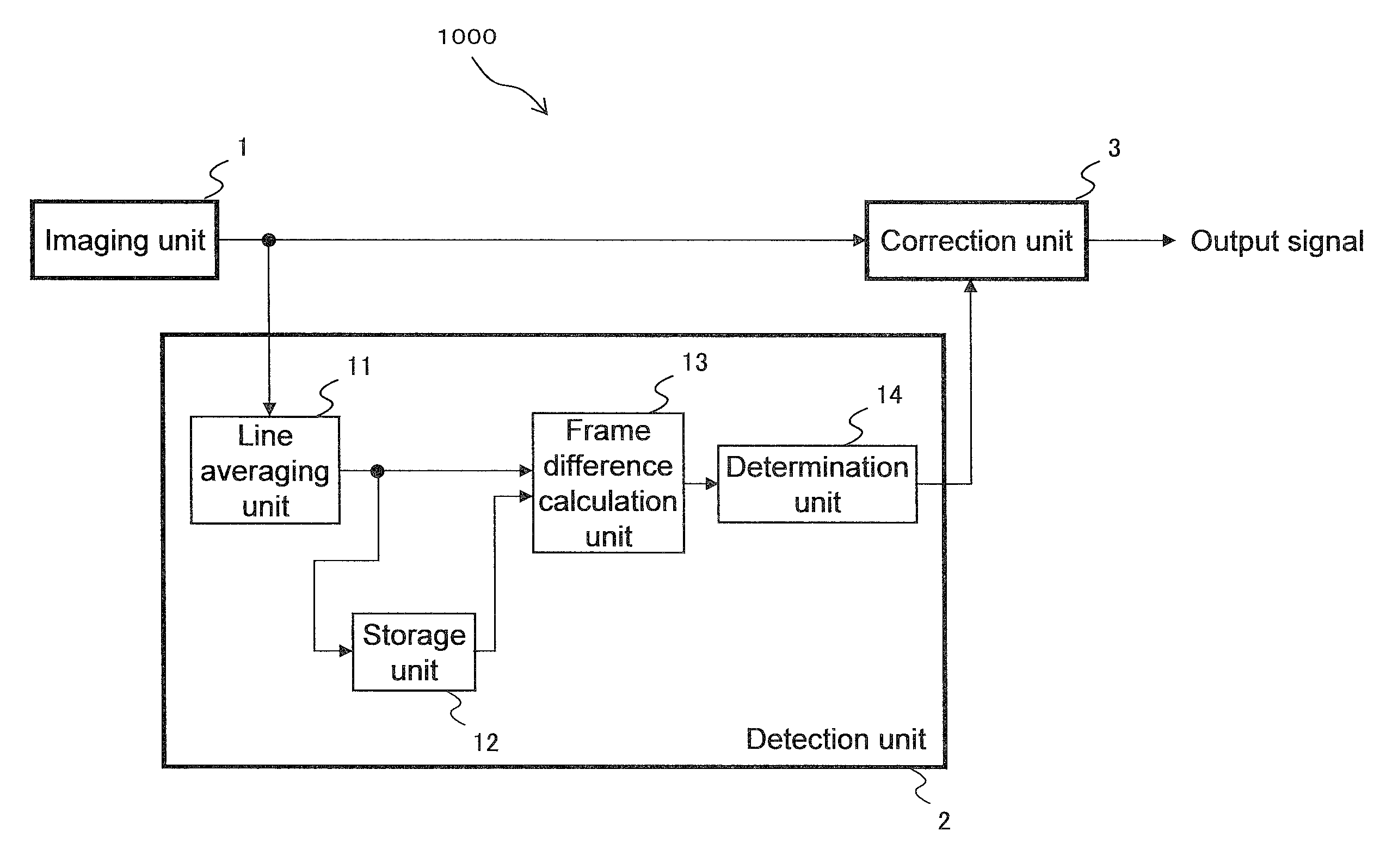
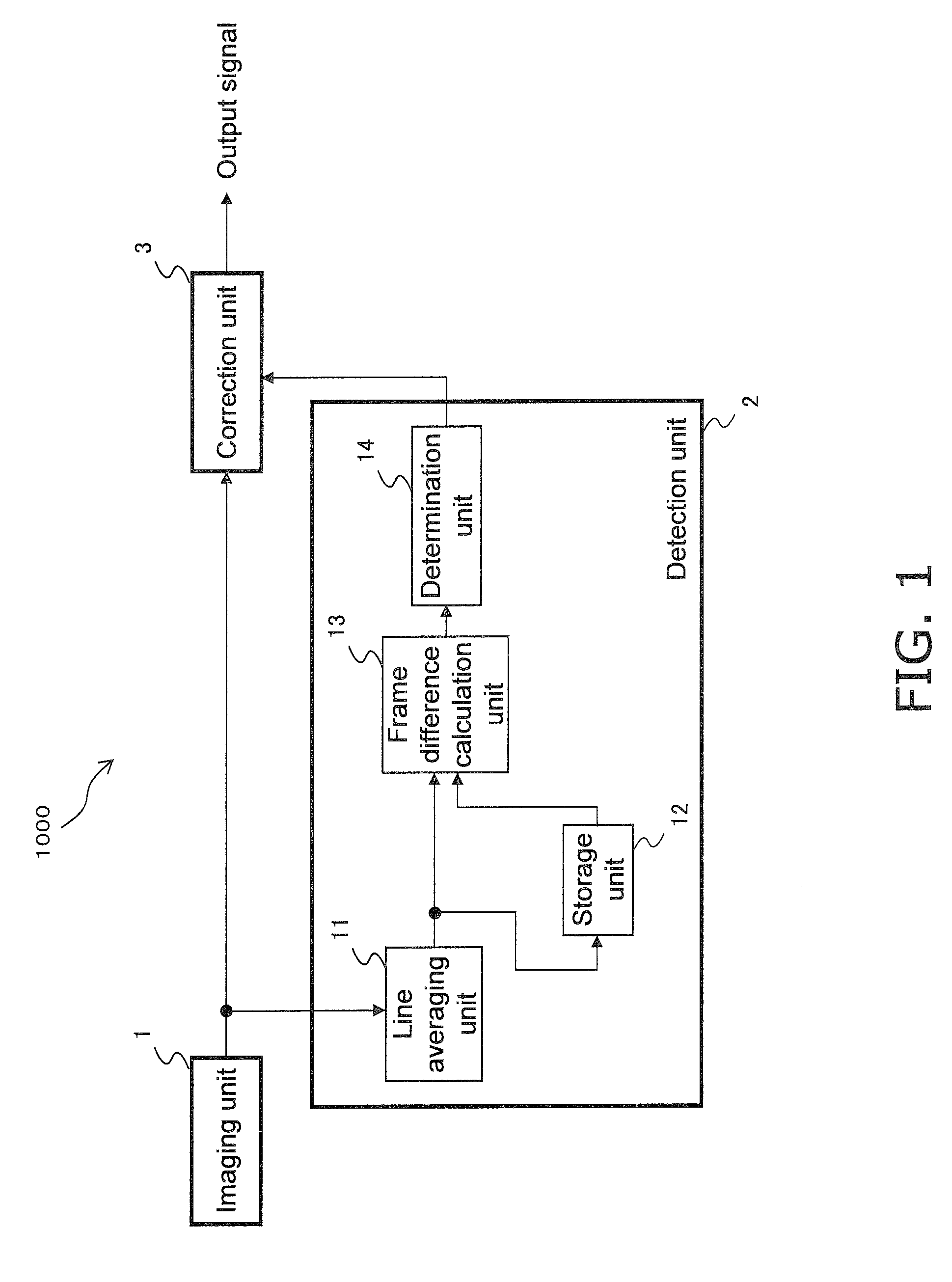
[0218]FIG. 1 is a diagram showing the schematic configuration of an imaging device 1000 of the first embodiment.

[0219]As shown in FIG. 1, the imaging device 1000 includes an imaging unit 1, a detection unit 2, and a correction unit 3.

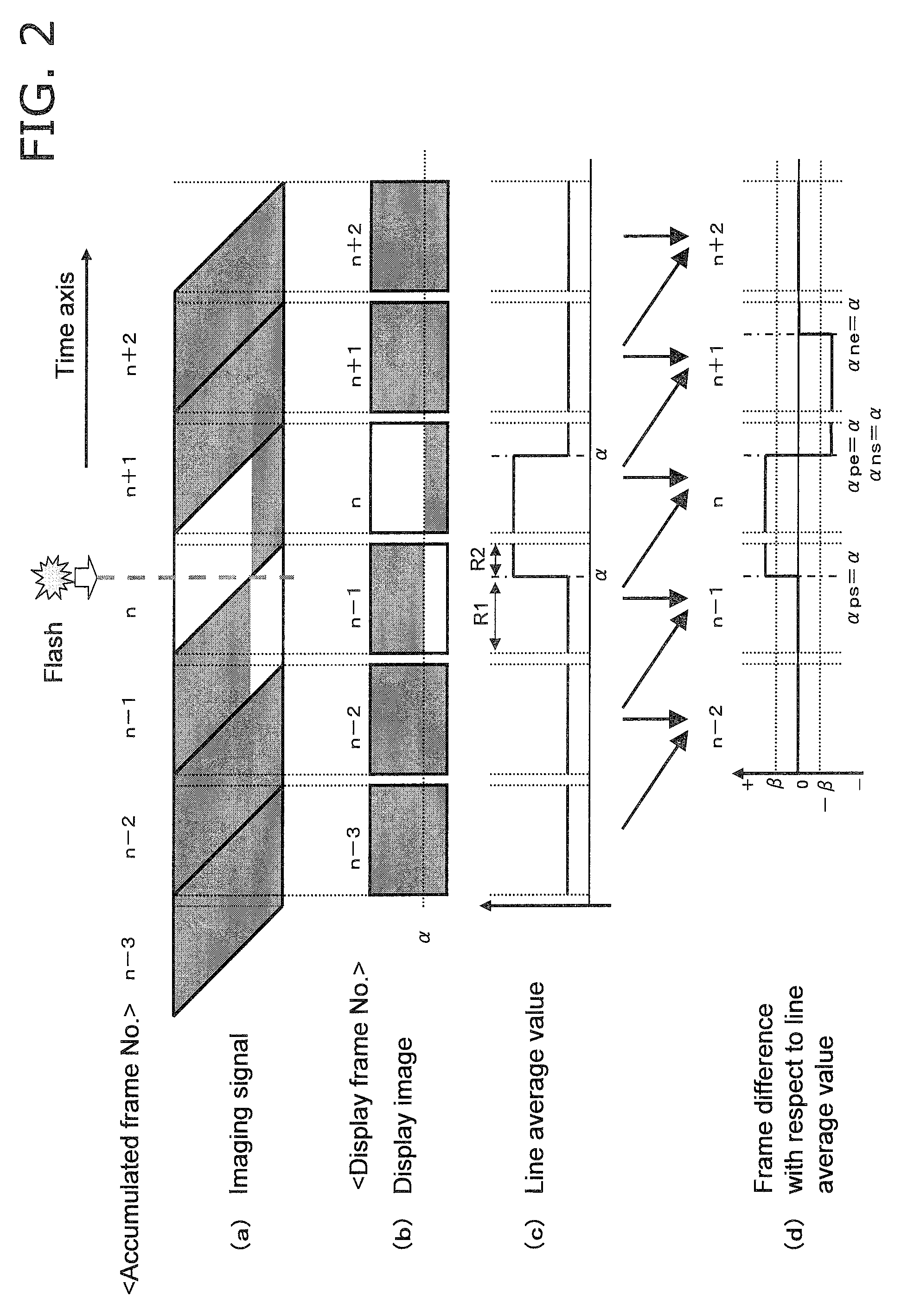
[0220]The imaging unit 1 is constituted including an imaging element such as a CMOS image sensor, and the imaging unit 1 acquires an imaging signal (video signal) by capturing images of a subject, and outputs the acquired imaging signal (video signal) to the detection unit 2 and the correction unit 3. Note that captured images (frame images) are formed by the imaging signal. The captured video can then be displayed by a display device by causing the display device to display a plurality of frame images.

[0221]As shown in FIG. 1, the detection unit 2 includes a line averaging unit 11 (line luminance information calculation unit), a storage unit 12, a frame difference calculation unit 13, and a determination unit 14. The detection unit 2 receives an ...

second embodiment

[0300]Next is a description of a second embodiment with reference to FIGS. 6 to 15.

[0301]

[0302]FIG. 6 is a diagram showing the schematic configuration of an imaging device 2000 of the second embodiment.

[0303]As shown in FIG. 6, the imaging device 2000 includes an imaging unit 1, a detection unit 4, and a flash correction processing unit 5.

[0304]The imaging unit 1 is constituted including an imaging element such as a CMOS image sensor, and the imaging unit 1 acquires an imaging signal (video signal) by capturing images of a subject, and outputs the acquired imaging signal (video signal) to the detection unit 4 and the flash correction processing unit 5. Note that in the present embodiment, it is assumed that the exposure time per frame of the imaging unit 1 is substantially the same as one frame period, which is determined by the imaging frame rate. For example, if the imaging frame rate is 60 frames / sec, one frame period and the exposure time are 1 / 60 sec.

[0305]The detection unit 4 ...

third embodiment

[0402]Next is a description of a third embodiment.

[0403]The configuration of an imaging device of the third embodiment is similar to the configuration of the imaging device 2000 of the second embodiment.

[0404]The following describes the imaging device of the third embodiment with reference to FIGS. 6, 7, 11, 12, and 13.

[0405]The operations of the evaluation value storage unit 412 and the evaluation value comparison unit 413 of the present embodiment differ from those of the second embodiment with respect to the following points (1) and (2). Specifically:

[0406](1) Out of the generated evaluation values, the evaluation value storage unit 412 temporarily stores the evaluation value of the top line.

[0407](2) The evaluation value comparison unit 413 compares the evaluation value of the top line that is stored in the evaluation value storage unit 412 and the evaluation value of the bottom line that was generated by the evaluation value generation unit 411, determines whether the influence...


PUM


Abstract

When capturing images of a subject with an imaging device that uses a CMOS image sensor, a white band-shaped artifact appears in the imaging signal due to the influence of a rolling shutter operation performed when an external flash has been emitted. Manipulating or removing images in which such an artifact appears requires specifying the frames in which the artifact appears. A line averaging unit (11) calculates the average luminance level of each line in the imaging signal, the average luminance levels are temporarily stored by a storage unit (12), and thereafter a frame difference calculation unit (13) calculates the difference between the line average luminance levels and the line average luminance levels of the next frame. These frame difference values are compared with a reference value, and it is determined that the influence of an external flash is present if a portion of interest with high values is continuous for one frame period.

Description

TECHNICAL FIELD[0001]The present invention relates to an imaging device that can mitigate white band-shaped artifacts that appear during the capturing of video due to the flash of a still camera or the like.BACKGROUND ART[0002]In recent years, imaging devices that use a CMOS (Complementary Metal Oxide Semiconductor) image sensor, which has features such as a small size, low power consumption, and high-speed imaging, have been making a breakthrough in the field of consumer video cameras and professional video cameras.[0003]A CMOS image sensor has various features that a CCD (Charge Coupled Device) does not have, and the method of reading out charge accumulated in photodiodes (hereinafter, “PD”) is also different between a CMOS image sensor and a CCD image sensor.[0004]With a CCD image sensor, PD charge readout is performed at the same time in all pixels, that is to say, using the so-called global shutter method. On the other hand, with a CMOS image sensor, PD charge readout is perfor...

Claims


Application Information

Patent Timeline
Patent Type & Authority Applications(United States)
IPC IPC(8): H04N9/73
CPCH04N5/2354G06T7/254H04N23/71H04N23/74
Inventor FUKUSHIMA, YASUSHIINOUE, TADAYUKIKINIWA, YUJIFUKUI, KATSUYUKI
Owner PANASONIC CORP
Why Eureka
Try Eureka