Semiconductor device, refresh control method thereof and computer system

a technology of a memory controller and a memory device, applied in the field of memory controller, can solve the problems of increasing consumption current and inability to apply to a general dram, and achieve the effects of reducing consumption current, rapid refresh operation, and improving memory access efficiency

Inactive Publication Date: 2011-09-15
PS4 LUXCO SARL
View PDF10 Cites 70 Cited by
  • Summary
  • Abstract
  • Description
  • Claims
  • Application Information

AI Technical Summary

Benefits of technology

[0015]According to the refresh control method of the semiconductor device of the invention, when receiving the refresh request for the refresh word line (refresh page) selected in the memory cell array, it is determined whether or not the word line in the active state (open page) exists in the unit area including the memory cell array. Then, if the open page does not exist, the refresh operation for the refresh page is performed, and if the open page exists, the open page is temporarily closed so that the refresh operation for the refresh page is performed, and thereafter the closed page is returned to an open state again. Thus, even if the refresh operation for the open page cannot immediately performed since the open page exists when an auto-refresh command is issued, a process of issuing another command by interrupting an auto refresh operation is not required, and thus the refresh operation for the refresh page can be rapidly completed within one refresh cycle.
[0017]According to the present invention, when receiving the refresh request of the memory cell array, the refresh operation for the refresh page can be reliably completed within one refresh cycle in a predetermined unit area having one page that can be opened in accordance with a situation whether a page that has already been opened exists or not, thereby suppressing an increase in consumption current. In this case, even when the predetermined unit area corresponds to one or more memory cell arrays or corresponds to one block (a plurality of memory cell arrays), the open page can be reliably determined so as to perform a rapid refresh operation. Further, in a semiconductor device having a multi-block configuration or having a multi-bank configuration, when performing the refresh operation in a situation where a page that has already been opened exists, it is not required to precharge bit lines in all areas, and also it is not required to issue a command for opening the page repeatedly, thereby improving memory access efficiency. As a result, it is possible to improve access efficiency of the DRAM employing open-page policy, and particularly a large effect can be obtained when the present invention is applied to a large capacity DRAM having a multi-core CPU.

Problems solved by technology

However, the control method disclosed in the Patent Reference 1 is applied to a memory operation in which all blocks (corresponding to banks of the DRAM) are always maintained in a page open state, and a problem arises in that it cannot be applied to a general DRAM.
Thus, this requires a complicated control using a plurality of commands, thereby causing a problem of an increase in consumption current.
Furthermore, in the control method disclosed in the Patent Reference 1, it is assumed that a memory controller issues a plurality of commands, and however a problem arises in that a new controller for the DRAM needs to be designed in order to maintain compatibility with the current DRAM that performs an auto-refresh operation by issuing one command.
In addition, the control method disclosed in the Patent Reference 2 has the same problems, and a control method capable of solving a series of these problems has not been proposed yet.

Method used


Image

  • Semiconductor device, refresh control method thereof and computer system
  • Semiconductor device, refresh control method thereof and computer system
  • Semiconductor device, refresh control method thereof and computer system

Examples


first embodiment

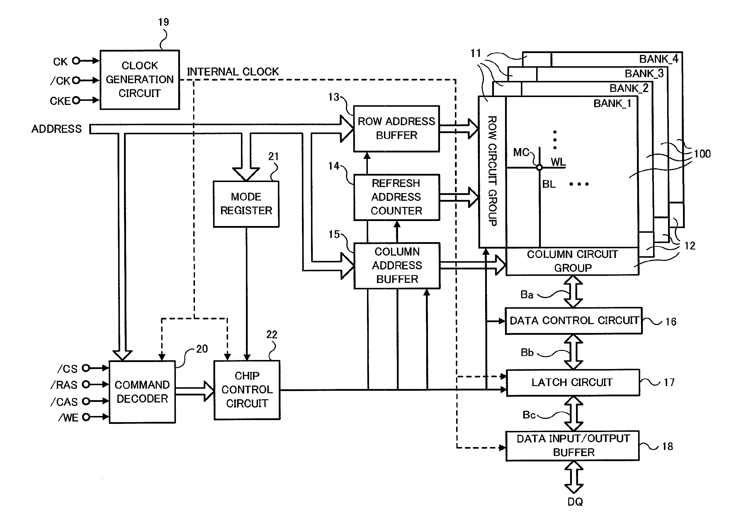
[0045]FIG. 1 shows a block diagram of an entire configuration of the DRAM of the first embodiment to which the present invention is applied. The DRAM shown in FIG. 1 is implemented on a memory chip C (FIG. 2), and is provided with a memory cell array region 100 divided into a plurality of banks (BANK), a row circuit group 11 and a column circuit group 12 that are attached to each bank. Although there are provided four banks (BANK) in the example of FIG. 1, the number of banks is not restricted. In the memory cell array region 100, a plurality of memory cells MC are formed at intersections of a plurality of word lines WL and a plurality of bit lines BL. The row circuit group 11 includes circuits such as a large number of row decoders (not shown) and the like that are provided corresponding to the plurality of word lines WL. The column circuit group 12 includes circuits such as later-described sense amplifier rows that are provided corresponding to the plurality of bit lines.

[0046]A r...

second embodiment

[0069]In the DRAM of the second embodiment, a relief circuit that replaces a defective word line with a redundancy word line is added to the DRAM of the first embodiment. The configurations and operations of FIGS. 1 to 5 and 8 to 10 in the first embodiment are common in the second embodiment and thus description thereof will be omitted. FIG. 11 is a flow chart showing a flow of the refresh control performed in the DRAM of the second embodiment. In FIG. 11, Step S20 is performed in the same manner as Step S10 in the first embodiment.

[0070]Subsequently, if the open page does not exist in the block BK (Step S20: NO) in accordance with determination result of Step S20, it is determined whether or not the refresh address matches a relief originating address (Step S21). The relief originating address means a row address at which a defective word line has existed and relieved. If the determination result of Step S21 indicates that the refresh address does not match the relief originating a...

third embodiment

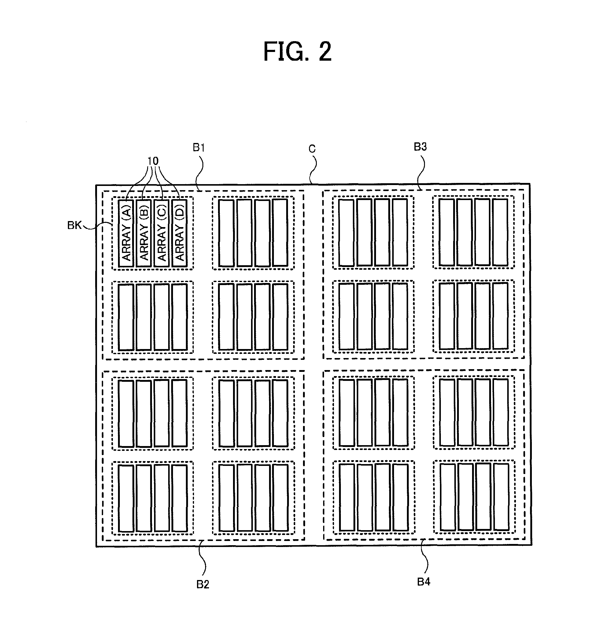
[0073]Although the refresh control corresponding to the existence of the open page is performed for each block BK in the DRAM of the first and second embodiments, the DRAM of the third embodiment is modified so that the same refresh control is performed for each memory cell array 10. FIG. 13 shows a first setting example of an array register AR (refer to FIG. 20) in the DRAM of the third embodiment. The array register AR is provided in the control data registers 40 of the array control circuit 32, and stores information required for performing the refresh control of the third embodiment. Specifically, when stored data in the memory cell MC corresponding to the open page is sensed and amplified by a predetermined sense amplifier SA, array address information identifying all memory cell arrays 10 to which word lines WL sharing the predetermined sense amplifier SA belong is stored in the array register AR.

[0074]Four memory cell arrays 10(A), 10(B), 10(C) and 10(D) are shown in the uppe...


PUM


Abstract

A semiconductor device comprises a first memory cell array, a register storing information of whether or not one of the word lines in an active state exists in a unit area and storing address information, and a control circuit controlling a refresh operation for a refresh word line based on the information in the register when receiving a refresh request. When the one of the word lines in an active state does not exist, memory cells connected to the refresh word line are refreshed. When the one of the word lines in an active state exists, the one of the word lines in an active state is set into an inactive state temporarily and the memory cells connected to the refresh word line are refreshed after precharging bit lines of the memory cells.

Description

BACKGROUND OF THE INVENTION[0001]1. Field of the Invention[0002]The present invention relates to a semiconductor device performing a refresh operation for a memory cell array including a plurality of memory cells, and particularly relates to a semiconductor device performing an auto-refresh operation in a situation where there is an open page in the memory cell array, and a refresh control method thereof.[0003]2. Description of Related Art[0004]In a semiconductor memory device such as a DRAM, a control for improving access efficiency has been introduced, in which a predetermined word line in a memory cell array is activated, data is sensed and amplified through a bit line (so-called “open page”) and this state is maintained. Meanwhile, when using the DRAM, for example, it is required to perform a refresh operation for retaining data of memory cells with a constant period. Conventionally, various control methods have been proposed for performing the refresh operation in the semicondu...

Claims


Application Information

Patent Timeline
Patent Type & Authority Applications(United States)
IPC IPC(8): G11C11/402G06F12/00
CPCG11C11/406G11C11/407G11C11/40618G11C11/40603
Inventor KAJIGAYA, KAZUHIKO
Owner PS4 LUXCO SARL
Why Eureka
Try Eureka