
Hysteresis Management in SOI Data Processing Circuits

a data processing circuit and hysteresis management technology, applied in error detection/correction, instruments, generating/distributing signals, etc., can solve the problems of increasing active and leakage power consumption, increasing wake-up time latency, and increasing the latency of point-to-point communication

Active Publication Date: 2012-02-02
ADVANCED MICRO DEVICES INC
View PDF2 Cites 2 Cited by
  • Summary
  • Abstract
  • Description
  • Claims
  • Application Information

AI Technical Summary

Benefits of technology

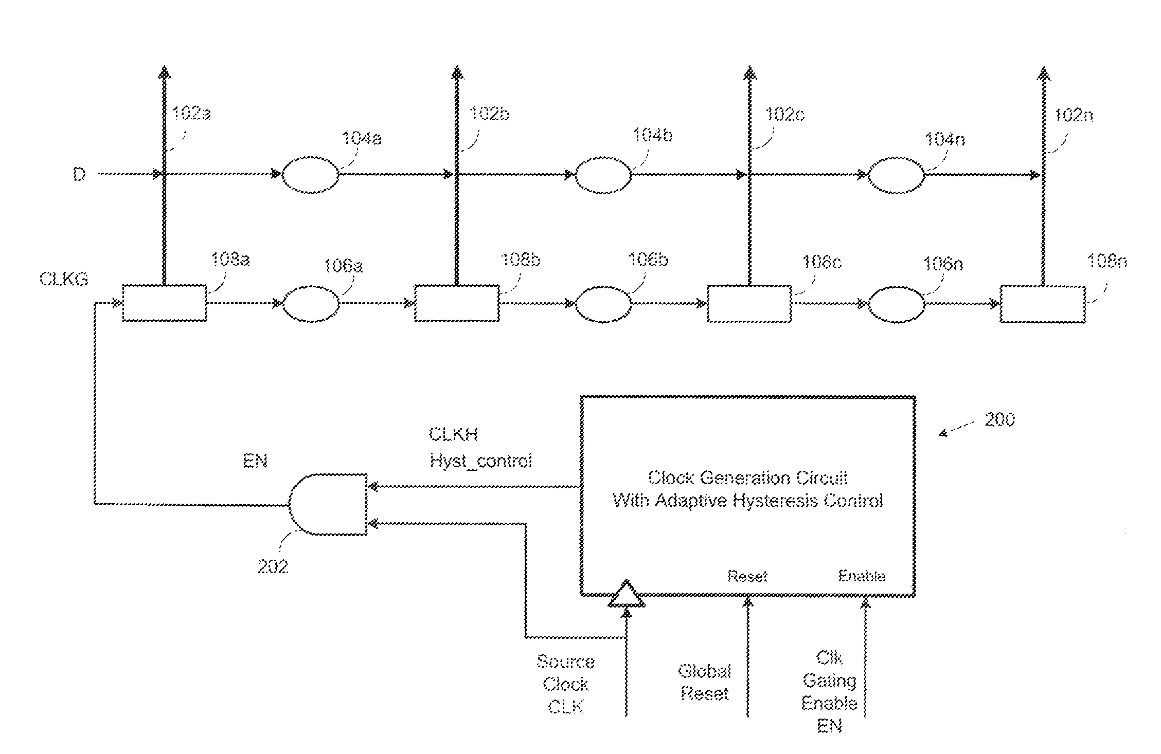
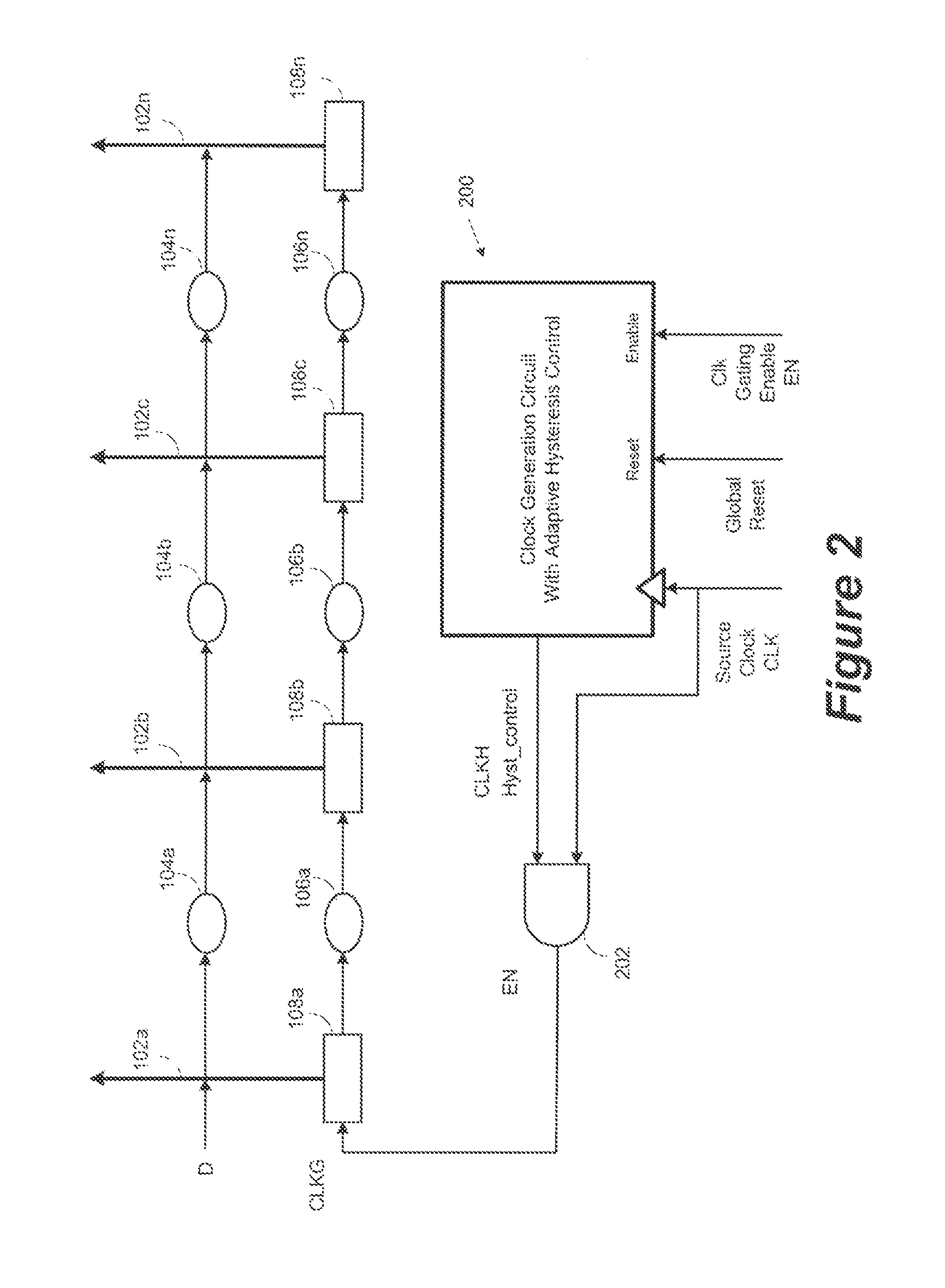
[0015]In one embodiment, the invention relates to a system for reducing the effects of hysteresis in a system for propagating data in a datapath. In this embodiment, the system comprises: a plurality of clocked data processing elements operable to receive input data and to generate output data therefrom; a clock generator operable to generate clock signals to propagate data through said data processing elements; and hysteresis management circuitry operable to mitigate hysteresis effects in said clock signals.
[0016]In another embodiment, the invention relates to a method for propagating data in a datapath. In this embodiment, the method comprises: using a plurality of clocked data processing elements to receive input data and to generate output data therefrom; using a clock generator to generate clock signals to propagate data through said data processing elements; and using hysteresis management circuitry to mitigate hysteresis effects in said clock signals.

Problems solved by technology

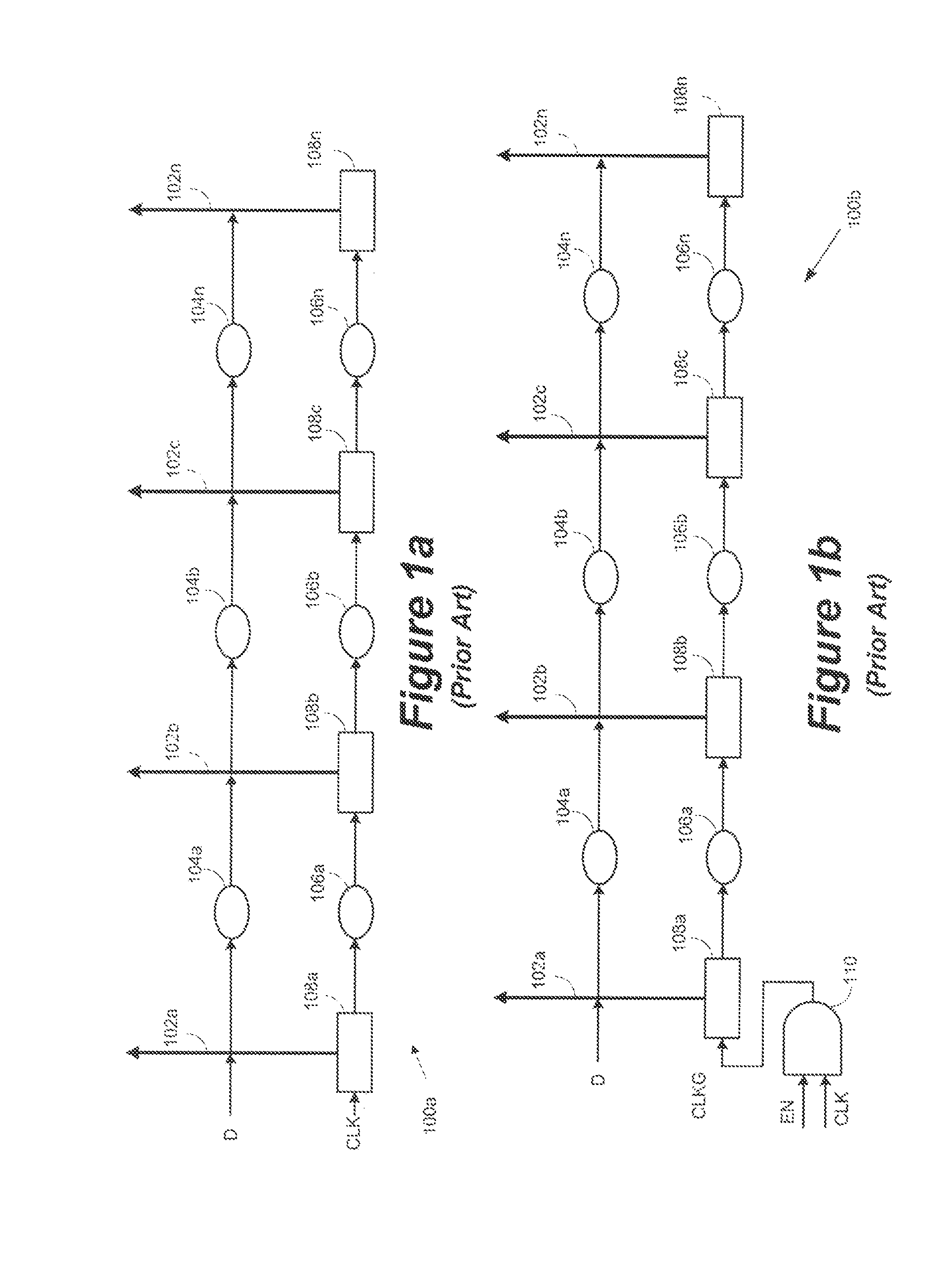
Therefore, in the design of SS channels in an SOI process, a significant amount of additional guard-band is added to cover for hysteresis-related effects that lead to increased latency of point-to-point communication, and increased active and leakage power consumption.
Likewise, in the design of a CMOS implementation in an SOI process, a significant amount of additional guard-band is added to cover for hysteresis-related effects that can lead to increased latency for wake-up period during chip initialization, point-to-point communication, increased active and leakage-power consumption.

Method used


Image

  • Hysteresis Management in SOI Data Processing Circuits
  • Hysteresis Management in SOI Data Processing Circuits
  • Hysteresis Management in SOI Data Processing Circuits

Examples


Embodiment Construction

[0014]Embodiments of the invention comprise systems and methods for improving data processing circuit performance by reducing the effects of hysteresis in SOI technology. Various embodiments of the invention are especially useful in source synchronous circuits; however, the techniques described herein are also applicable to other forms of data processing circuits.

[0015]In one embodiment, the invention relates to a system for reducing the effects of hysteresis in a system for propagating data in a datapath. In this embodiment, the system comprises: a plurality of clocked data processing elements operable to receive input data and to generate output data therefrom; a clock generator operable to generate clock signals to propagate data through said data processing elements; and hysteresis management circuitry operable to mitigate hysteresis effects in said clock signals.

[0016]In another embodiment, the invention relates to a method for propagating data in a datapath. In this embodiment...


PUM


Abstract

Embodiments of systems and methods are described for reducing the effects of hysteresis in the operation of data processing circuitry. In this embodiment of the invention, adaptive control circuitry is used to reduce the effects of hysteresis. The embodiment disclosed herein provides significant reduction in the effects of hysteresis and, therefore, a significant reduction in the amount of guard band needed to compensate for hysteresis effects in SOI processes and thereby improving the performance / power characteristics of the circuit.

Description

BACKGROUND OF THE INVENTION[0001]1. Field of the Invention[0002]The present invention relates in general to the field of data processing circuitry and, more specifically, to systems and methods for improving data processing circuit performance by reducing the effects of hysteresis in Silicon on Insulator (SOI) technology.[0003]2. Description of the Related Art[0004]Source Synchronous Bus (SSB) timing is a technique typically used to distribute high speed data from one point of the chip to another. In source synchronous (SS) channels, one or multiple data streams are bundled together with a clock signal that are all generated in a transmitter circuit and travel through long distances on-chip to a receiver circuit that uses the same clock to capture the sent data. SS methodology is an extremely robust distribution technique, as it allows cancellation of all forms of systematic variations that affect both the data and clock lines.[0005]In SOI, over the usual sources of process variatio...

Claims


Application Information

Patent Timeline
Patent Type & Authority Applications(United States)
IPC IPC(8): G06F1/04
CPCG06F2213/0038G06F1/10
Inventor IYER, ARUNTOMAR, BHAWNAJAIN, ANIMESHLEELA, KRISHNA SETHUPATHY
Owner ADVANCED MICRO DEVICES INC
Learn More