Semiconductor device

a technology of semiconductor devices and shielding circuits, applied in the direction of electrical equipment, instruments, computing, etc., can solve the problems of unintentionally short communication distance, rfid malfunction, deterioration or damage of components provided in rfid, etc., to achieve high reliability of semiconductor devices, reduce power consumption of protection circuits, and reduce power consumption. the effect of protection circuits

Inactive Publication Date: 2012-02-09
SEMICON ENERGY LAB CO LTD
View PDF25 Cites 30 Cited by
  • Summary
  • Abstract
  • Description
  • Claims
  • Application Information

AI Technical Summary

Benefits of technology

[0011]It is an object of one embodiment of the present invention to provide a highly reliable semiconductor device (an RFID) including a protection circuit which operates normally even when the communication distance is extremely short and which consumes little power when the communication distance is long.
[0012]One embodiment of the present invention employs the following configuration to achieve the above object. In other words, a feature of one embodiment of the present invention is to provide a protection circuit for protecting an element which is included in a semiconductor device (an RFID) capable of wirelessly communicating data. The protection circuit is designed to operate when the level of a DC power supply potential which is generated in a rectifier circuit is equal to or greater than a predetermined level (a reference level), so as to decrease the level of the generated DC power supply potential. On the other hand, the protection circuit is designed not to operate when the DC power supply potential which is generated in the rectifier circuit is equal to or less than the predetermined level (the reference level), so as to use the generated DC power supply potential without change. A transistor of the protection circuit includes an oxide semiconductor layer, which enables a reduction in the off-state current of the transistor and a reduction in power consumption of the protection circuit.
[0020]A semiconductor device (an RFID) including a protection circuit according to one embodiment of the present invention can protect an internal element from high power which is received by the RFID, even when the communication distance is extremely short. In addition, the semiconductor device can suppress power consumption of the protection circuit when the communication distance is long. Thus, it is possible to provide a highly reliable semiconductor device because the protection circuit operates normally even when the communication distance is extremely short and the power consumption of the protection circuit is low even when the communication distance is long.

Problems solved by technology

When the RFID is supplied with high power, the RFID might malfunction because of incorrect demodulation of signals from the reader / writer, or elements provided in the RFID might be deteriorated or damaged.
In view of the foregoing actual uses of such a wireless communication system, the communication distance might be extremely short unintentionally, and as a result, high power might be supplied to an RFID.

Method used


Image

  • Semiconductor device
  • Semiconductor device
  • Semiconductor device

Examples


embodiment 1

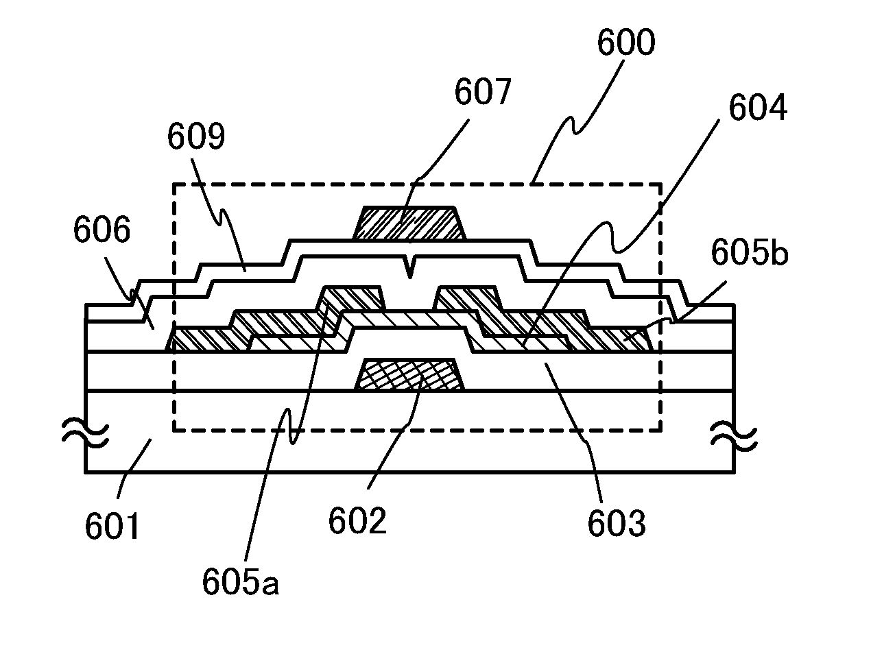
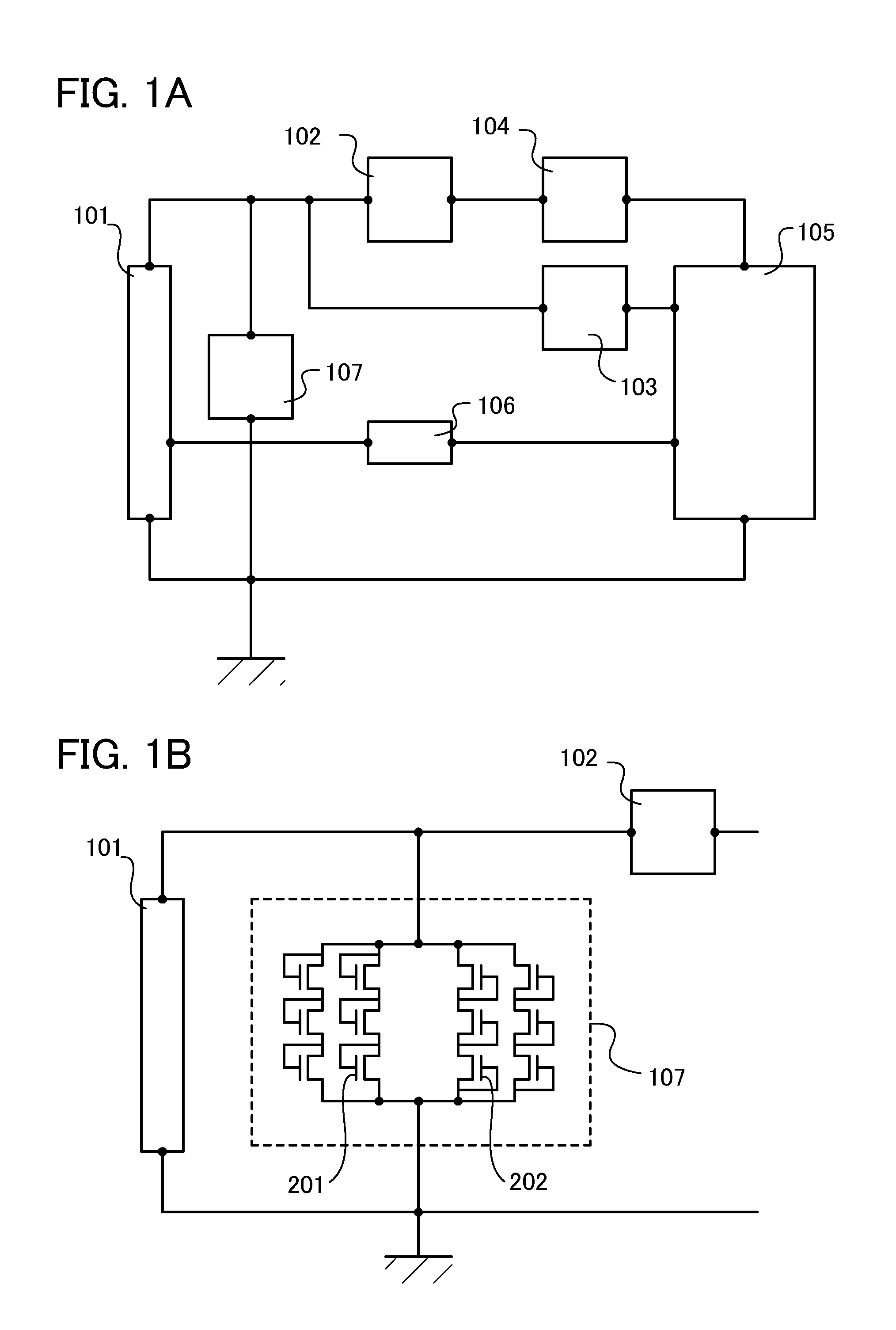
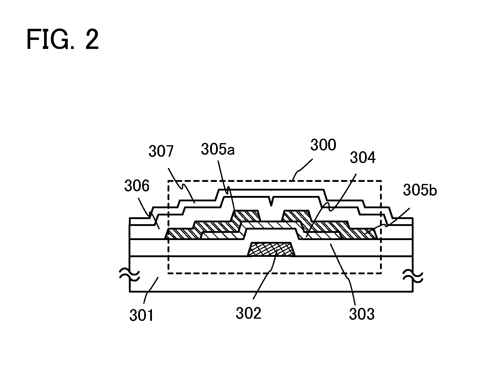
[0033]In this embodiment, circuits which can be used for a semiconductor device of the present invention are described with reference to FIGS. 1A and 1B and FIG. 2.

[0034]FIG. 1A is a block diagram illustrating a configuration of a semiconductor device. The semiconductor device includes the following components: an antenna 101 which receives a carrier wave or an amplitude-modulated wave; a rectifier circuit 102 which generates an internal voltage Vin by rectifying the carrier wave or the amplitude-modulated wave received by the antenna 101; a demodulation circuit 103 which generates an internal signal by demodulating the carrier wave or the amplitude-modulated wave received by the antenna 101; a constant voltage circuit 104 which outputs as a power supply voltage Vdd a constant voltage obtained from the internal voltage Vin generated by the rectifier circuit 102; a logic circuit 105 which analyzes the power supply voltage Vdd generated by the constant voltage circuit 104 and a signal...

embodiment 2

[0059]In this embodiment, a configuration in which circuits that can be used for an antenna, a rectifier circuit, and a protection circuit differ from those in Embodiment 1 is described with reference to FIGS. 3A and 3B and FIGS. 4A and 4B.

[0060]Circuits that can be used for a semiconductor device of the present invention are described below with reference to FIGS. 3A and 3B.

[0061]FIG. 3A is a block diagram illustrating a configuration of a semiconductor device. The semiconductor device includes the following components: an antenna 401 which receives a carrier wave or an amplitude-modulated wave; a rectifier circuit 402 which generates an internal voltage Vin by rectifying the carrier wave or the amplitude-modulated wave; a demodulation circuit 403 which generates an internal signal by demodulating the carrier wave or the amplitude-modulated wave received by the antenna 401; a constant voltage circuit 404 which outputs as a power supply voltage Vdd a constant voltage obtained from t...

embodiment 3

[0088]In this embodiment, a configuration in which circuits that can be used for an antenna, a rectifier circuit, and a protection circuit differ from those in Embodiments 1 and 2 is described with reference to FIGS. 5A and 5B.

[0089]A configuration of a protection circuit illustrated in FIGS. 5A and 5B is described in detail below.

[0090]FIG. 5A is a block diagram illustrating a configuration of a semiconductor device. The semiconductor device includes the following components: an antenna 701 which receives a carrier wave or an amplitude-modulated wave; a rectifier circuit 702 which generates an internal voltage Vin by rectifying the carrier wave or the amplitude-modulated wave; a demodulation circuit 703 which generates an internal signal by demodulating the carrier wave or the amplitude-modulated wave received by the antenna 701; a constant voltage circuit 704 which outputs as a power supply voltage Vdd a constant voltage obtained from the internal voltage Vin generated by the rect...


PUM


Abstract

A protection circuit is designed to operate when the level of a DC power supply potential which is generated in a rectifier circuit is equal to or greater than a predetermined level (a reference level), so as to decrease the level of the generated DC power supply potential. On the other hand, the protection circuit is designed not to operate when the DC power supply potential which is generated in the rectifier circuit is equal to or less than the predetermined level (the reference level), so as to use the generated DC power supply potential without change. A transistor of the protection circuit includes an oxide semiconductor layer, which enables a reduction in the off-state current of the transistor and a reduction in power consumption of the protection circuit.

Description

BACKGROUND OF THE INVENTION[0001]1. Field of the Invention[0002]The present invention to be disclosed in this specification relates to a semiconductor device capable of communicating (transmitting and receiving) data wirelessly (a data carrier). In particular, the present invention relates to a protection circuit which prevents breakage or deterioration of elements which are included in a semiconductor device when the semiconductor device receives high power in wireless communication.[0003]2. Description of the Related Art[0004]In recent years, individual identification technologies have attracted attention. In these technologies, an identification (ID) number is assigned to each object to recognize the history of information on the object and to be utilized in production, management, or the like. In particular, radio-frequency identification (RFID) techniques for transmitting and receiving data by wireless communication have been widely used. A wireless communication system using t...

Claims


Application Information

Patent Timeline
Patent Type & Authority Applications(United States)
IPC IPC(8): H04Q5/22
CPCH04Q2213/13095G06K19/07
Inventor KAMATA, KOICHIRO
Owner SEMICON ENERGY LAB CO LTD
Why Eureka
Try Eureka