Semiconductor device and driving method thereof

a technology of semiconductor devices and drives, applied in the direction of solid-state devices, digital storage, instruments, etc., can solve the problems of increased cost per storage capacity, difficulty in reducing power consumption, stored data,

Inactive Publication Date: 2012-02-09
SEMICON ENERGY LAB CO LTD
View PDF1 Cites 40 Cited by
  • Summary
  • Abstract
  • Description
  • Claims
  • Application Information

AI Technical Summary

Benefits of technology

[0012]In view of the above problems, an object of one embodiment of the present invention is to provide a semiconductor device with a n

Problems solved by technology

For that reason, another writing operation (refresh operation) is necessary at predetermined intervals, and it is difficult to sufficiently reduce power consumption.
Further, since stored data is lost when power supply stops, an additional storage device using a magnetic material or an optical material is needed in order to hold the data for a long time.
However, cost per storage capacity is increased because a circuit such as a flip-flop is used.
Moreover, as in a DRAM, stored data in an SRAM is lost when power supply stops.
However, a gate insulating layer included in a storage element deteriorates by tunneling current generated in writing, so tha

Method used


Image

  • Semiconductor device and driving method thereof
  • Semiconductor device and driving method thereof
  • Semiconductor device and driving method thereof

Examples


embodiment 1

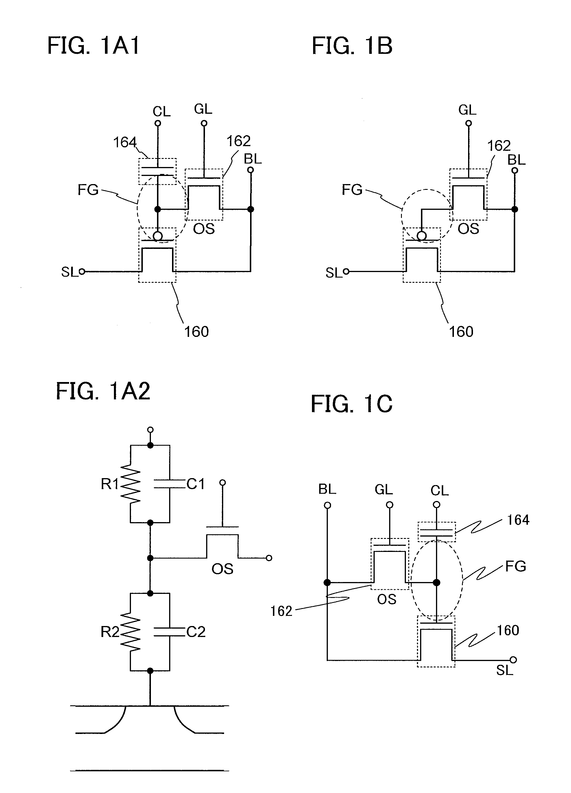
[0079]In this embodiment, a basic circuit configuration and operation of a semiconductor device according to one embodiment of the present invention will be described with reference to FIGS. 1A1, 1A2, 1B, and 1C. Note that in each of circuit diagrams, in some cases, “OS” is written beside a transistor in order to indicate that the transistor includes an oxide semiconductor.

[0080]First, the most basic circuit configuration and its operation will be described with reference to FIGS. 1A1, 1A2, 1B, and 1C. In a semiconductor device illustrated in FIG. 1A1, a bit line BL, a source electrode (or a drain electrode) of a transistor 160, and a source electrode (or a drain electrode) of a transistor 162 are electrically connected to each other. A source line SL is electrically connected to the drain electrode (or the source electrode) of the transistor 160. A gate line GL is electrically connected to a gate electrode of the transistor 162. A gate electrode of the transistor 160 and the drain ...

application example

[0111]Next, a more specific circuit configuration to which the circuit illustrated in FIGS. 1A1, 1A2, 1B, and 1C is applied and an operation thereof will be described with reference to FIG. 2, FIGS. 3A and 3B1 to 3B5, FIGS. 4A and 4B, FIGS. 5A and 5B, FIGS. 6A and 6B, FIGS. 7A and 7B, FIG. 8, FIGS. 9A and 9B, FIG. 10, FIG. 11, FIG. 12, FIG. 13, FIG. 14, FIG. 15, and FIG. 16. In this embodiment, a so-called multi-valued memory which holds a plurality of states in one memory cell is described

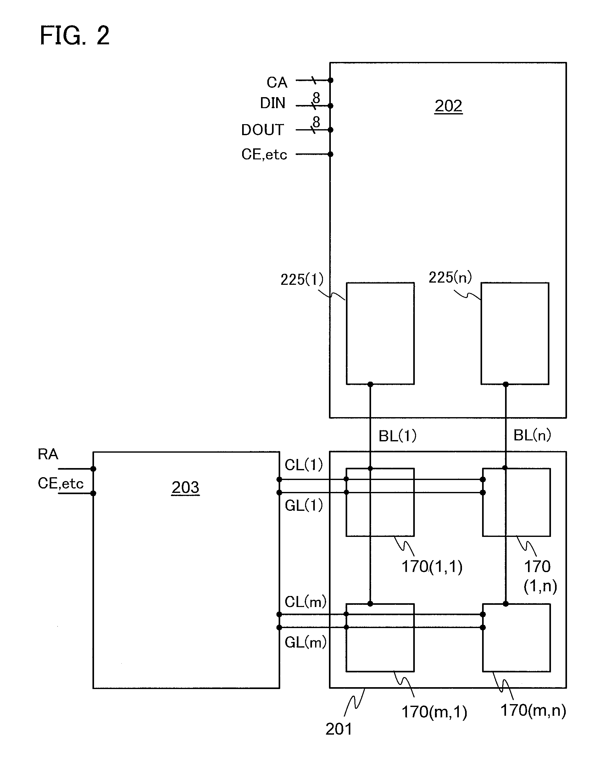
[0112]FIG. 2 is an example of a block diagram of a semiconductor device. A feature of a block diagram illustrated in FIG. 2 relates to writing operation of a driver circuit. A semiconductor device illustrated in FIG. 2 is a multi-valued memory which holds 2k-valued (k is an integer greater than or equal to 1) state in one memory cell and includes a memory cell array 201 including a plurality of memory cells, a column driver circuit 202, and a row driver circuit 203.

[0113]The memory cell array 201 ...

embodiment 2

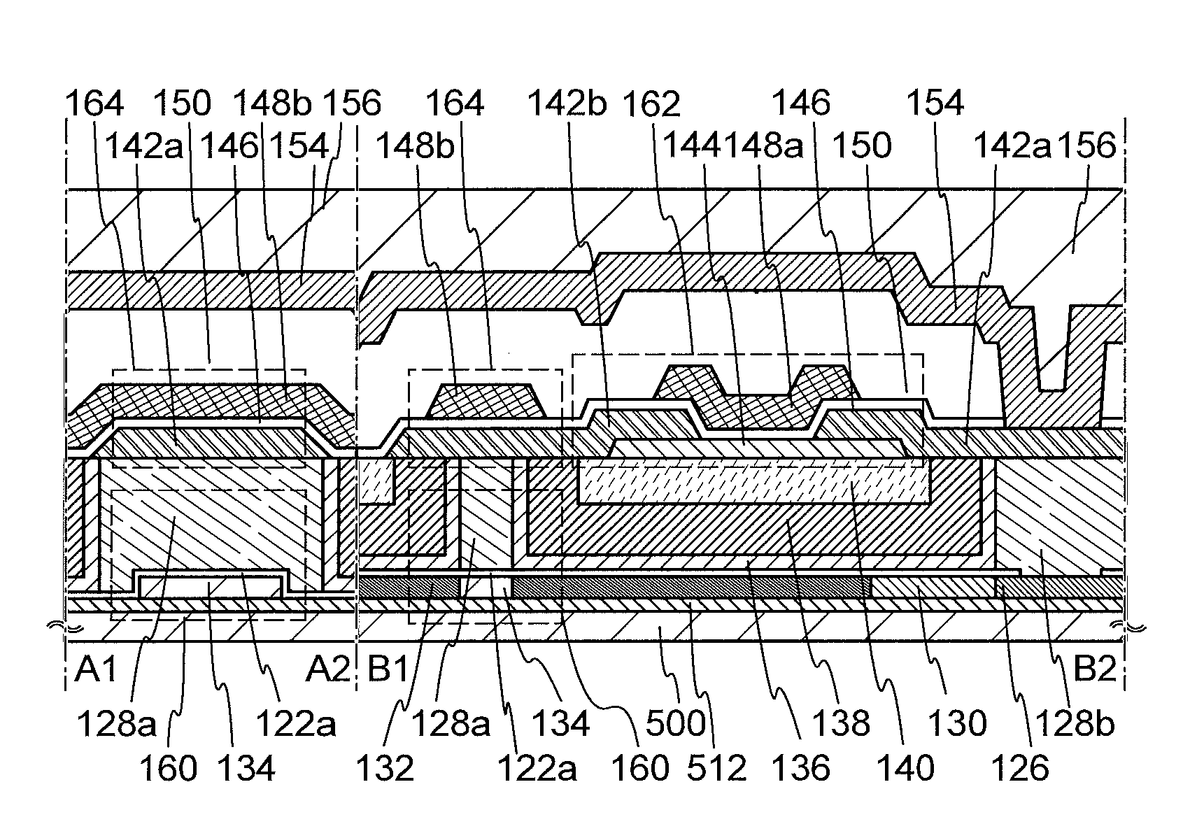
[0210]In this embodiment, a structure of a semiconductor device and a method for manufacturing the semiconductor device according to one embodiment of the present invention will be described with reference to FIGS. 17A and 17B, FIGS. 18A to 18G, FIGS. 19A to 19E, FIGS. 20A to 20D, FIGS. 21A to 21D, and FIGS. 22A to 22C.

[0211]FIGS. 17A and 17B illustrate an example of a structure of a semiconductor device. FIG. 17A illustrates a cross section of the semiconductor device, and FIG. 17B illustrates a plan view of the semiconductor device. Here, FIG. 17A corresponds to the cross section along lines A1-A2 and B1-B2 in FIG. 17B. The semiconductor device illustrated in FIGS. 17A and 17B includes a transistor 160 including a first semiconductor material in a lower portion, and a transistor 162 including a second semiconductor material in an upper portion. Here, the first semiconductor material is preferably different from the second semiconductor material. For example, a semiconductor materi...


PUM


Abstract

A semiconductor device including a memory cell formed using a wide bandgap semiconductor, for example, an oxide semiconductor is provided. The semiconductor device includes a potential change circuit having a function of outputting a potential lower than a reference potential for reading data from the memory cell. With the use of the wide bandgap semiconductor, an off-state current of a transistor included in the memory cell can be sufficiently reduced, and the semiconductor device which can hold data for a long period can be provided.

Description

BACKGROUND OF THE INVENTION[0001]1. Field of the Invention[0002]The present invention relates to a semiconductor device using a semiconductor element and a method for driving the semiconductor device.[0003]2. Description of the Related Art[0004]Storage devices using semiconductor elements are broadly classified into two categories: a volatile device that loses stored data when power supply stops, and a non-volatile device that holds stored data even when power is not supplied.[0005]A typical example of a volatile storage device is a dynamic random access memory (DRAM). A DRAM stores data in such a manner that a transistor included in a storage element is selected and charge is accumulated in a capacitor.[0006]When data is read from a DRAM, charge in a capacitor is lost on the above-described principle; thus, another writing operation is necessary whenever data is read. A data holding period is short because charge flows from / into a transistor forming a memory element by leakage curr...

Claims


Application Information

Patent Timeline
IPC IPC(8): G11C11/24H01L27/108H01L27/092
CPCG11C16/0433G11C16/26H01L21/76254G11C11/403H01L27/1156H01L27/1225H01L27/11517H10B41/00H10B41/70H10B99/00H10B12/00
Inventor NAGATSUKA, SHUHEIMATSUZAKI, TAKANORI
Owner SEMICON ENERGY LAB CO LTD
Why Eureka
Try Eureka