Chip scale package and fabrication method thereof

Active Publication Date: 2012-02-16
SILICONWARE PRECISION IND CO LTD
View PDF48 Cites 41 Cited by
  • Summary
  • Abstract
  • Description
  • Claims
  • Application Information

AI Technical Summary

Benefits of technology

[0023]Therefore, the present invention mainly involves forming conductive elements on conductive pads of a first wiring layer of a hard board; forming an encapsulating layer on the hard board to encapsulate the conductive elements; disposing an electronic component on the encapsulating layer and pressing the electronic component and the hard board so as to attach the inactive surface of the electronic component to the hard board and removing a portion of the encapsulating layer by laser to expose the surfaces of the conductive elements and the active surface of the electronic component; and sequentially forming a first dielectric layer and a third wiring layer on the encapsulating layer. Therein, the third wiring layer is electrically con

Problems solved by technology

However, the application of the RDL technique or disposing of conductive traces on the chip is limited by the size of the chip or the area of the active surface of the chip.
Particularly, as chips are developed towards high integration and compact size, they do not have enough surface area for mounting of more solder balls for electrical connection to an external device.
However, since the chip 12 is fixed by being attached to the adhesive film 11, deviation of the chip 12 can easily occur due to film-softening and extension caused by heat, especially in the molding process, thus adversely affecting the electrical connection between the electrode pads 120 of the chip 12 and the wiring layer 15 during the subsequent RDL process.
Referring to FIG. 2, since the adhesive film 11 is softened by heat in the molding process, overflow 130 of the encapsulant 13 can easily occur to the active surface 121 of the chip 1

Method used


Image

  • Chip scale package and fabrication method thereof
  • Chip scale package and fabrication method thereof
  • Chip scale package and fabrication method thereof

Examples


Embodiment Construction

[0032]The following illustrative embodiments are provided to illustrate the disclosure of the present invention, these and other advantages and effects can be apparent to those in the art after reading this specification.

[0033]FIGS. 4A to 4F are cross-sectional views showing a fabrication method of a chip scale package according to the present invention, wherein FIG. 4F′ is another embodiment of FIG. 4F.

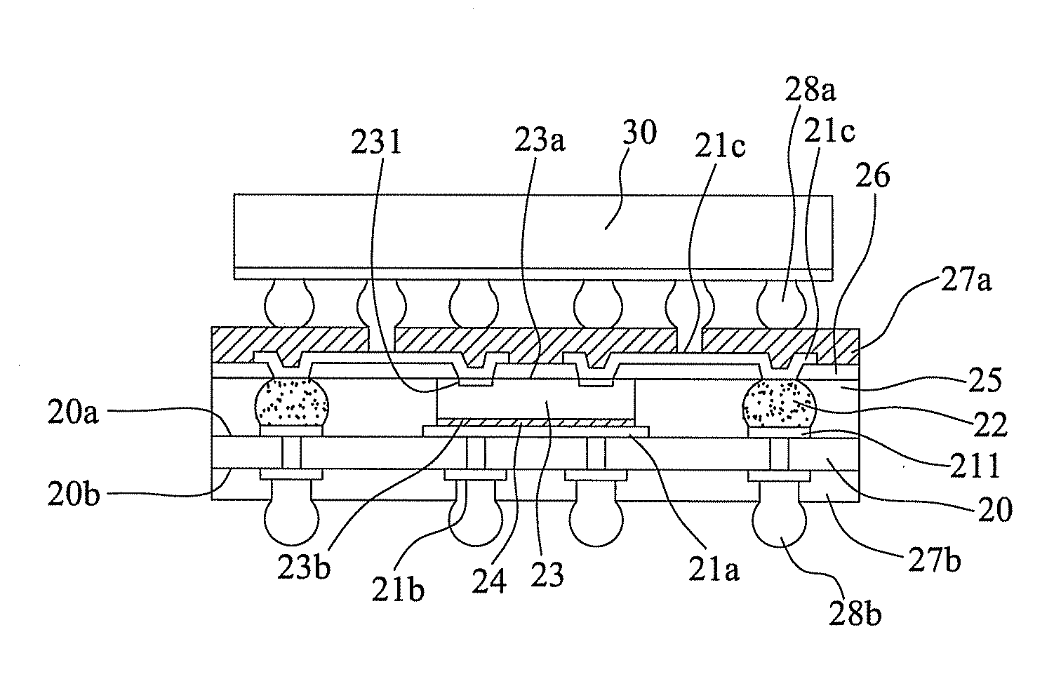
[0034]Referring to FIG. 4A, a hard board 20 having a first surface 20a and an opposite second surface 20b is provided, which can be made of a copper clad laminate (CCL) with two or more layers. A first wiring layer 21a and a second wiring layer 21b are respectively disposed on the first surface 20a and the second surface 20b of the hard board 20 and electrically connected to each other. The first wiring layer 21a has a plurality of conductive pads 211 and at least a heat dissipation pad 212 for dissipating heat of an electronic component subsequently mounted thereon.

[0035]Referring t...


PUM


Abstract

A CSP includes: a hard board having a first wiring layer with conductive pads; a plurality of conductive elements disposed on at least a portion of the conductive pads; an electronic component having opposite active and inactive surfaces and being mounted on the hard board via the inactive surface; an encapsulating layer disposed on the hard board for encapsulating the conductive elements and electronic component, the active surface of the electronic component and the surfaces of the conductive elements being exposed through the encapsulating layer; a first dielectric layer and a third wiring layer disposed on the encapsulating layer, the third wiring layer being electrically connected to the conductive elements and the electronic component and further electrically connected to the first wiring layer through the conductive elements, thereby obtaining a stacked connection structure without the need of PTHs and using the hard board as a main structure to avoid warpage.

Description

BACKGROUND OF THE INVENTION[0001]1. Field of the Invention[0002]The present invention relates generally to semiconductor packages and fabrication methods thereof, and more particularly, to a chip scale package (CSP) and a fabrication method thereof.[0003]2. Description of Related Art[0004]A chip scale package is characterized in that the package size is equivalent to the size of the chip that is disposed in the package. U.S. Pat. No. 5,892,179, No. 6,103,552, No. 6,287,893, No. 6,350,668 and No. 6,433,427 disclose a conventional CSP structure, wherein a build-up structure is directly formed on a chip without using a chip carrier, such as a substrate or a lead frame, and a redistribution layer (RDL) technique is used to accomplish a redistribution of the electrode pads of the chip to a desired pattern.[0005]However, the application of the RDL technique or disposing of conductive traces on the chip is limited by the size of the chip or the area of the active surface of the chip. Parti...

Claims


Application Information

Patent Timeline
IPC IPC(8): H01L23/488H01L21/44
CPCH01L23/3128H01L24/19H01L24/20H01L24/24H01L24/25H01L24/32H01L24/73H01L24/82H01L25/105H01L2224/12105H01L2224/24225H01L2224/25171H01L2224/32155H01L2224/73267H01L2225/1058H01L2924/01029H01L2924/01082H01L2924/15311H01L2924/01033H01L2924/014H01L2224/32225H01L2924/3511H01L2225/1035H01L2224/92244H01L2225/1041
Inventor CHANG, CHIANG-CHENGHUANG, CHIEN-PINGKE, CHUN-CHILIAO, HSIN-YIHSU, HSI-CHANG
Owner SILICONWARE PRECISION IND CO LTD
Why Eureka
Try Eureka