Organic el device, method of producing organic el device, and electronic apparatus

a technology of organic el and electronic equipment, which is applied in the manufacture of electric discharge tubes/lamps, instruments, discharge tubes luminescnet screens, etc., can solve the problems of low heat resistance and increase production costs, and achieve the effect of improving display quality and reducing light emission

Active Publication Date: 2012-02-16
SEIKO EPSON CORP
View PDF13 Cites 50 Cited by
  • Summary
  • Abstract
  • Description
  • Claims
  • Application Information

AI Technical Summary

Benefits of technology

[0029]With such a production method, it is possible to form at least a further transparent coloring layer throughout the light shielding area. Accordingly, it is

Problems solved by technology

However, in the production process of the above-described organic EL device, a process of forming a metal thin film and a patterning process are additionally necessar

Method used


Image

  • Organic el device, method of producing organic el device, and electronic apparatus
  • Organic el device, method of producing organic el device, and electronic apparatus
  • Organic el device, method of producing organic el device, and electronic apparatus

Examples


first embodiment

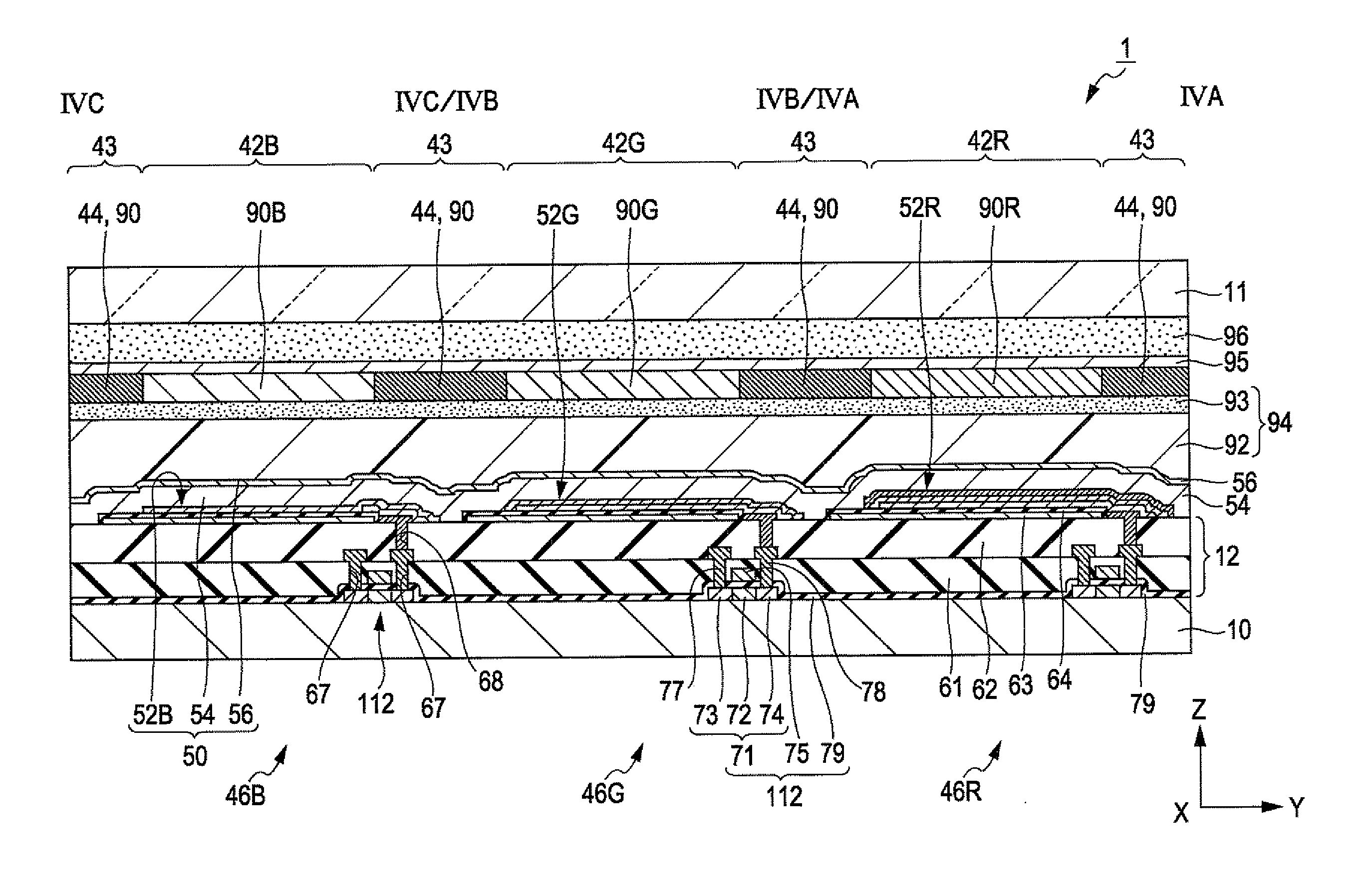
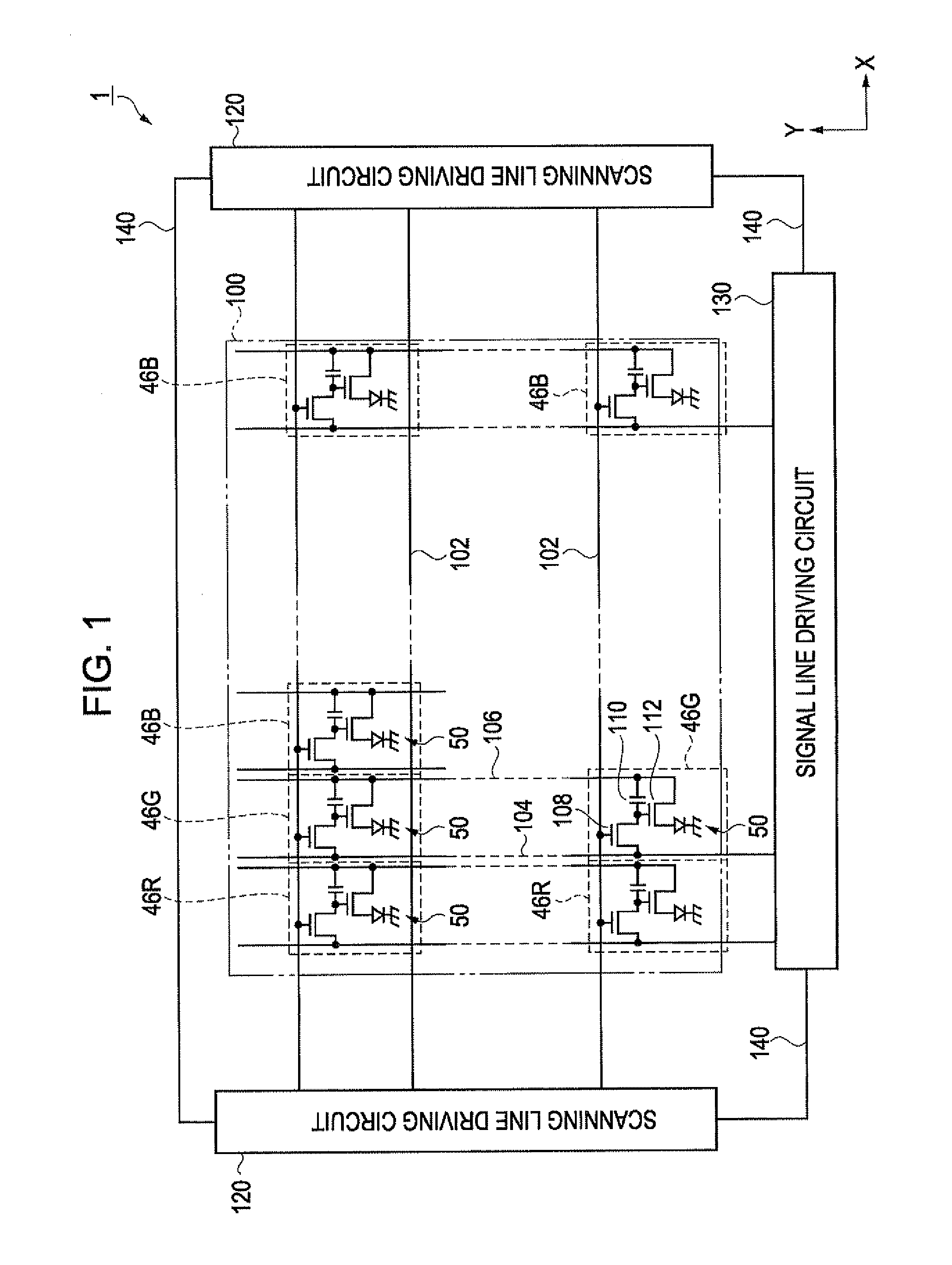
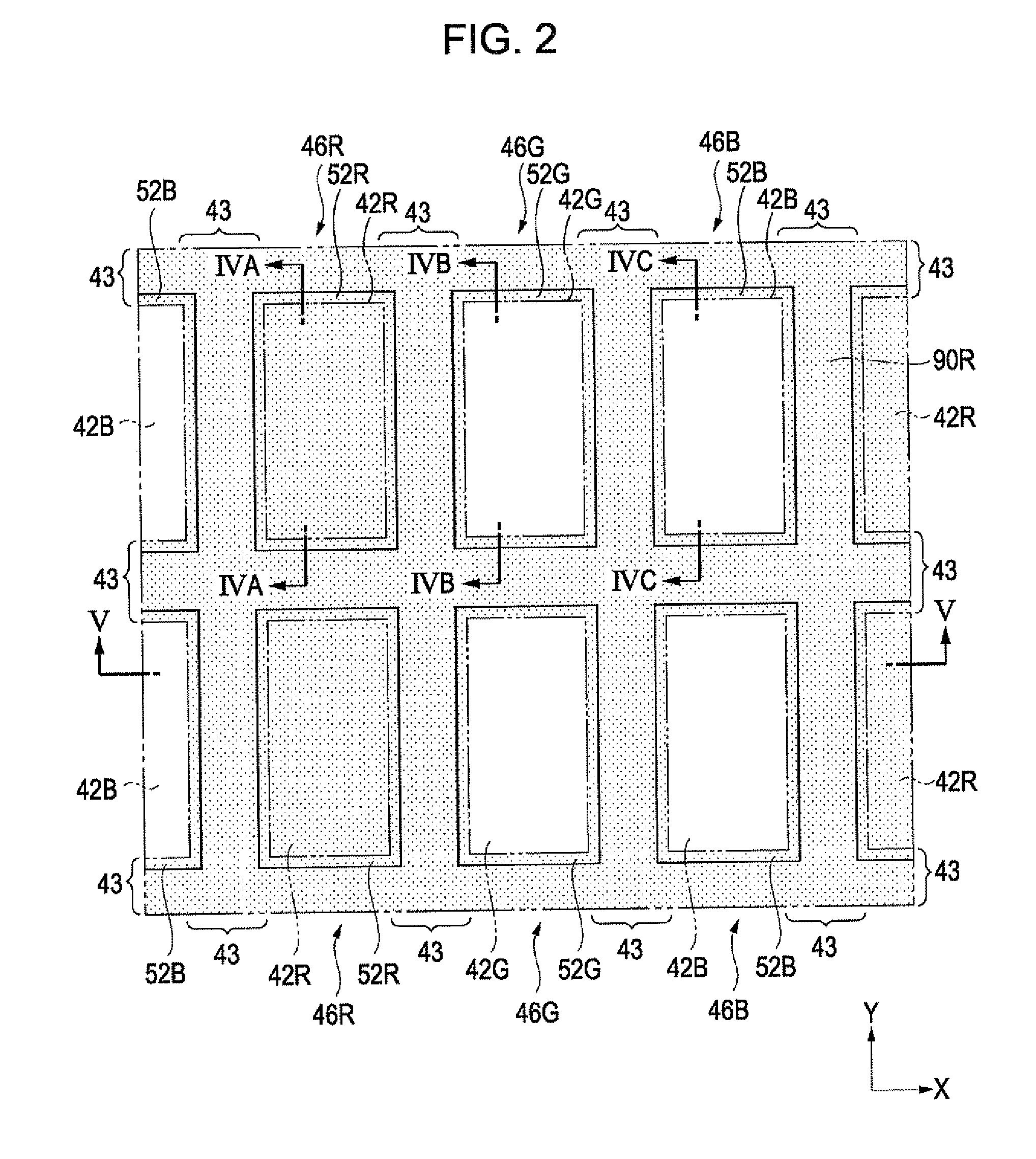
[0048]FIG. 1 is a diagram illustrating a circuit configuration of an organic EL device 1 according to the embodiment. A circuit configuration of organic EL devices according to embodiments to be described later is the same as the configuration shown in FIG. 1. The organic EL device 1 is an active matrix type organic EL device which individually controls emitting light of a plurality of regularly formed organic EL elements 50 to form a color image in an image display area 100. In the image display area 100, a plurality of scanning lines 102 extending in the X direction, a plurality of signal lines 104 extending in the Y direction to perpendicularly intersect with the scanning lines, and a plurality of power supply lines 106 extending in parallel to the signal lines are formed. A pixel 46 is formed in each section surrounded with three kinds of lines.

[0049]Each pixel 46 is provided with a switching TFT (thin film transistor) 108 in which a scanning signal is supplied to a gate electro...

second embodiment

[0105]An organic EL device as an electro-optic device according to a second embodiment of the invention will be described with reference to FIG. 8 to FIG. 10. FIG. 8 is a schematic plan view illustrating an arrangement of pixels 46, pixel electrodes 52, and the like in the image display area 100 (see FIG. 1) of the organic EL device 2, and an area where the color filter 90 is formed, according to the second embodiment. The organic EL device 2 according to the embodiment has a configuration similar to that of the organic EL device 1 of the first embodiment. A configuration of the element layer 12 and the like is the same, and a configuration of the color filter 90 and the partition 44 and the distance of the pixel electrodes 52 in the Y direction are different from those of the organic EL device 1. The same reference numerals and signs are given to the common constituent elements, and a part of description thereof is omitted. A circuit diagram and a cross-sectional view in the Y dire...

third embodiment

[0116]Next, an organic EL device as an electro-optic device according to a third embodiment of the invention will be described. FIG. 11 is a schematic plan view illustrating arrangement of pixels 46 and pixel electrodes 52 in an image display area 100 (see FIG. 1) of an organic EL device 3 according to the third embodiment, and an area where color filters 90 are formed. The organic EL device 3 according to the embodiment has a configuration similar to the organic EL device 1 and the organic EL device 2 described above, and there is a difference in the configuration of the (widely defined) color filter 90 and the partition 44. The same reference numerals and signs are given to the common constituent elements, a part of description thereof is omitted, and a circuit diagram and a cross-sectional view in the Y direction are not shown. A cross-sectional view in the X direction of the organic EL device 3 according to the embodiment is substantially the same as the cross-sectional view of ...


PUM


Abstract

An organic EL device includes a substrate, an organic EL element that is formed on the substrate and is provided with a first electrode, a light emitting functional layer, and a second electrode having transparent conductivity to emit light to the second electrode side, a color filter that is formed on the second electrode side in a pixel area where the organic EL element emits the light, and a partition that is formed in a light shielding area that is an area other than the pixel area. The color filter is provided with any one of a red color filter, a green color filter, and a blue color filter. At least one color filter of the three color filters constitutes at least a part of the partition.

Description

BACKGROUND[0001]1. Technical Field[0002]The present invention relates to an organic EL device, a method of producing the organic EL device, and an electronic apparatus.[0003]2. Related Art[0004]Recently, as a flat display device, attention has been paid to an organic EL device in which organic EL elements formed by laminating an anode (first electrode), a light emitting functional layer including at least an organic EL (electroluminescent) layer, and a cathode (second electrode) are regularly arranged in an image display area. Fields requiring miniaturization such as a display screen for a mobile phone, a head mount display (HMD), and an electronic viewfinder (EVF) have been developed as fields of use for the organic EL device. In the small-size organic EL device, to reduce matching deviation between the organic EL element and a color filter, employing an on-chip color filter in which the color filter is formed on a substrate on which the organic EL element is formed can be consider...

Claims


Application Information

Patent Timeline
IPC IPC(8): H01J1/62H01J9/18
CPCH01L27/322H01L51/5284H10K59/38H10K50/865G02B5/201H10K59/30H10K50/125
Inventor HANAMURA, YUKIIWATA, SHINICHIIWASAKI, MASANORINISHIOKA, DAISUKE
Owner SEIKO EPSON CORP
Why Eureka
Try Eureka