
Image Sensor Package with Dual Substrates and the Method of the Same

a dual-substrat, image sensor technology, applied in the direction of semiconductor devices, semiconductor/solid-state device details, electrical apparatus, etc., can solve the problems of low noise performance, inability to meet the demand of producing smaller chips with high-density elements on the chip, etc., to achieve the effect of improving reliability, shrinking device size, and increasing electrical conductivity

Active Publication Date: 2012-02-23
YANG CHING LUNG
View PDF8 Cites 34 Cited by
  • Summary
  • Abstract
  • Description
  • Claims
  • Application Information

AI Technical Summary

Benefits of technology

[0011]The further object of the present invention is to provide an image sensor package with dual substrate having die opening window to improve the reliability and shrinking the device size.
[0012]The further object of the present invention is to provide an image sensor package with dual substrates which have lower and upper wiring patterns by copper clad laminated (CCL) and E-plating Cu / Au or Cu / Ni / Au metal for increasing electrical conductivity.

Problems solved by technology

As a semiconductor become more complicated, the traditional package technique, for example lead frame package, flex package, rigid package technique, can't meet the demand of producing smaller chip with high density elements on the chip.
In a large number of image sensors, a photodiode structure called a pinned or a buried photodiode is used because of its low noise performance.
Although these methods eliminate the difficulties associated with wire bonding, however, the PCB's is very large with respect to the size of the image sensor chip and the transparent cover.
Moreover, the conductive film risks interference with sensing circuitry on the image sensor chip and requires the formation of dummy leads or dam structures to compensate for this problem.
Thus, the thickness of the substrate is unlikely to be scaled down due to the structure has ball high and extruding die receiving structure which limits the scale of the package shrinkage.
The prior art suffers complicated processes to form the image package and the package structure is too high and unable to be scaled down.

Method used


Image

  • Image Sensor Package with Dual Substrates and the Method of the Same
  • Image Sensor Package with Dual Substrates and the Method of the Same
  • Image Sensor Package with Dual Substrates and the Method of the Same

Examples


Embodiment Construction

[0022]The invention will now be described in greater detail with preferred embodiments of the invention and illustrations attached. Nevertheless, it should be recognized that the preferred embodiments of the invention is only for illustrating. Besides the preferred embodiment mentioned here, present invention can be practiced in a wide range of other embodiments besides those explicitly described, and the scope of the present invention is expressly not limited expect as specified in the accompanying Claims.

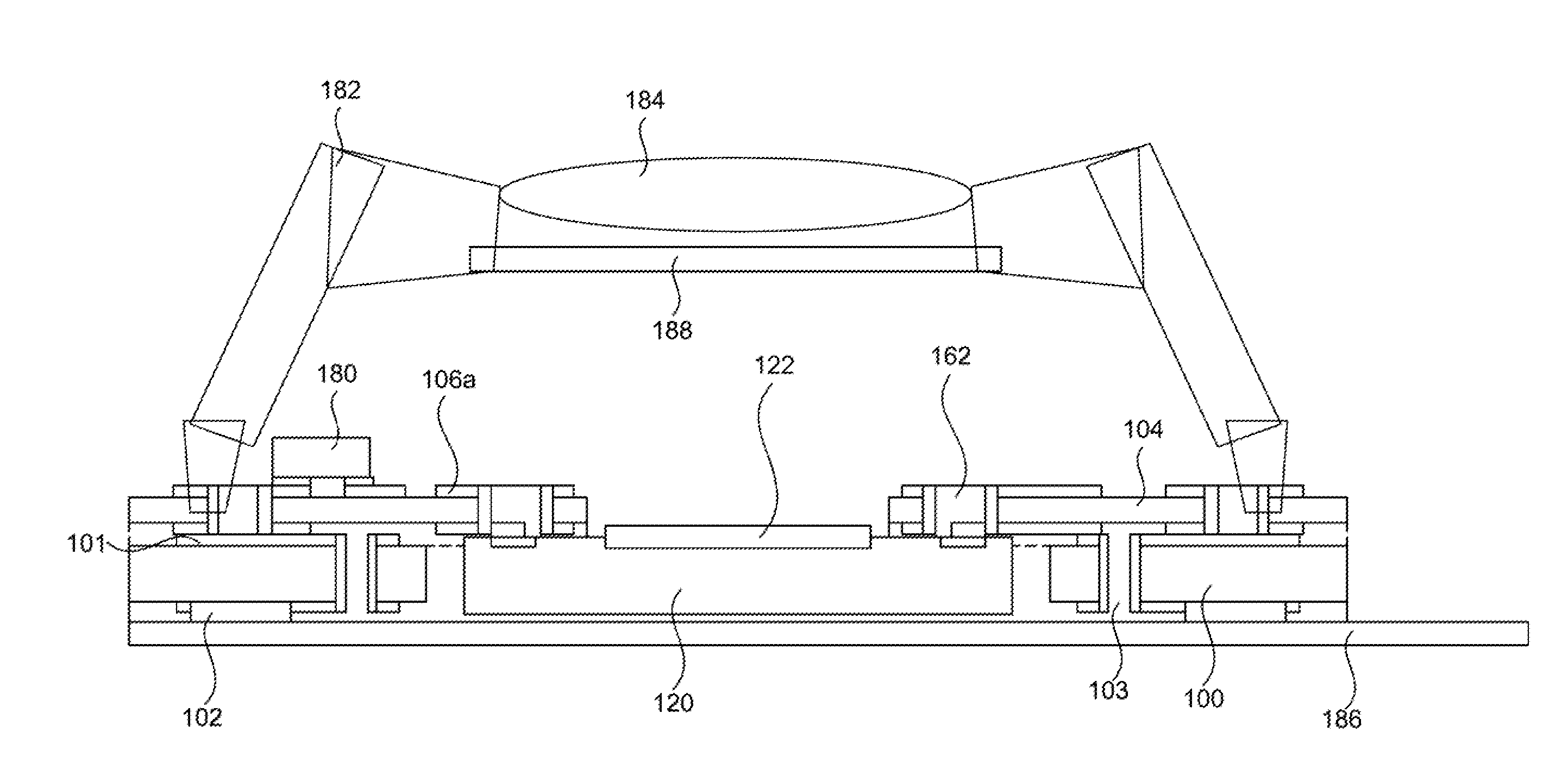
[0023]The present invention discloses a substrate structure with die (or multi-chips) embedded and dual build-up layers formed over the both side-surfaces, shown in FIGS. 6 and 7, and it illustrates a cross sectional view of system in package (SIP) structure which includes a substrate having die embedded inside with dual layers and passive components, WL-CSP, CSP, BGA, Flip Chip etc. surface mounting on top build up layers and terminal pins on opposite side according to the presen...


PUM


Abstract

The image sensor package with dual substrates comprises a first substrate with a die receiving opening and a plurality of first through hole penetrated through the first substrate; a second substrate with a die opening window and a plurality of second through hole penetrated through the second substrate, formed on the first substrate. A part of the second wiring pattern is coupled to a part of the third wiring pattern; an image die having conductive pads and sensing array received within the die receiving opening and the sensing array being exposed by the die opening window; and a through hole conductive material refilled into the plurality of second through hole, some of the plurality of second through hole coupling to the conductive pads of the image sensor.

Description

[0001]The invention is relative to Continuation-In-Part (CIP) of application Ser. No. 12 / 232,847 that filing on date Sep. 25, 2008 by the inventor.FIELD OF THE INVENTION[0002]This invention relates to an image sensor package, and more particularly to an image sensor package with dual substrates having die embedded therein.DESCRIPTION OF THE PRIOR ART[0003]In the field of semiconductor devices, the device density is increased and the device dimension is reduced, continuously. The demand for the packaging or interconnecting techniques in such high density devices is also increased to fit the situation mentioned above. Conventionally, in the flip-chip attachment method, an array of solder bumps is formed on the surface of the die. The formation of the solder bumps may be carried out by using a solder composite material through a solder mask for producing a desired pattern of solder bumps. The function of chip package includes power distribution, signal distribution, heat dissipation, p...

Claims


Application Information

Patent Timeline
Patent Type & Authority Applications(United States)
IPC IPC(8): H01L31/0232
CPCH01L24/24H01L24/82H01L2924/10253H01L27/14618H01L27/14625H01L2224/24225H01L2224/82039H01L2924/01013H01L2924/01029H01L2924/01075H01L2924/01077H01L2924/01078H01L2924/01079H01L2924/01082H01L2924/09701H01L2924/14H01L2924/15311H01L2924/19041H01L2924/19043H01L2924/01033H01L2924/014H01L24/16H01L2924/19105H01L2924/00H01L2924/12043H01L2924/15788H01L2924/351
Inventor YANG, WEN-KUN
Owner YANG CHING LUNG
Features
  • Generate Ideas
  • Intellectual Property
  • Life Sciences
  • Materials
  • Tech Scout
  • Unparalleled Data Quality
  • Higher Quality Content
  • 60% Fewer Hallucinations
Learn More