CDM-resilient high voltage ESD protection cell

a high-voltage esd protection and cdm-resilient technology, applied in emergency protective circuit arrangements, transistors, etc., can solve problems such as not being the case, and achieve the effect of reducing the voltage to the control gate and avoiding cdm stress damag

Inactive Publication Date: 2012-03-01
NAT SEMICON CORP
View PDF3 Cites 7 Cited by
  • Summary
  • Abstract
  • Description
  • Claims
  • Application Information

AI Technical Summary

Benefits of technology

[0006]Further, according to the invention, there is provided a method of avoiding CDM stress damage in an ESD clamp with high side high voltage avalanche diode reference providing a voltage reference to a control gate of the ESD clamp, comprising providing the control gate with a resistor between the control gate and the avalanche diode reference, to reduce the voltage to the control gate. The method may comprise connecting a reverse path diode between the control gate and ground.

Problems solved by technology

However, while these devices work well for relatively low frequency pulses such as the 100 ns human body model (HBM) pulses, this is not the case with very fast TLP (of the order of 2 ns), as defined by the charged device model (CDM) pulse.

Method used


Image

  • CDM-resilient high voltage ESD protection cell
  • CDM-resilient high voltage ESD protection cell

Examples


Embodiment Construction

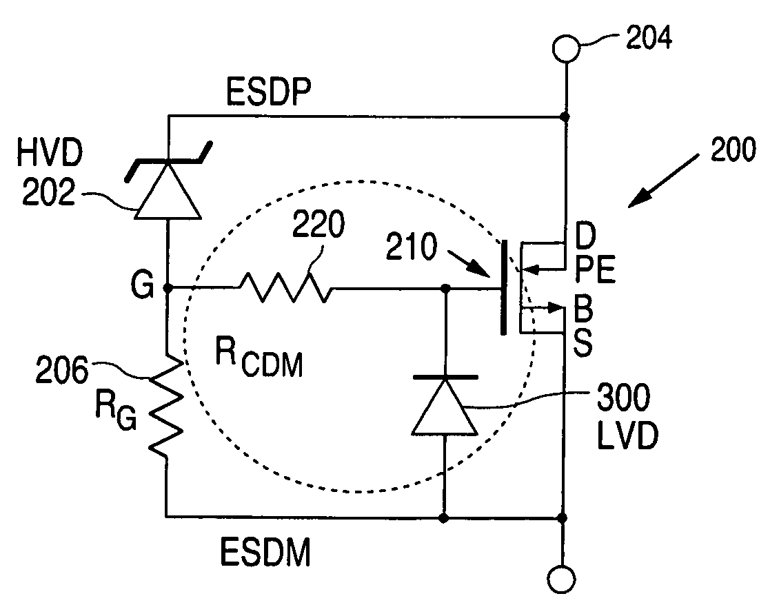
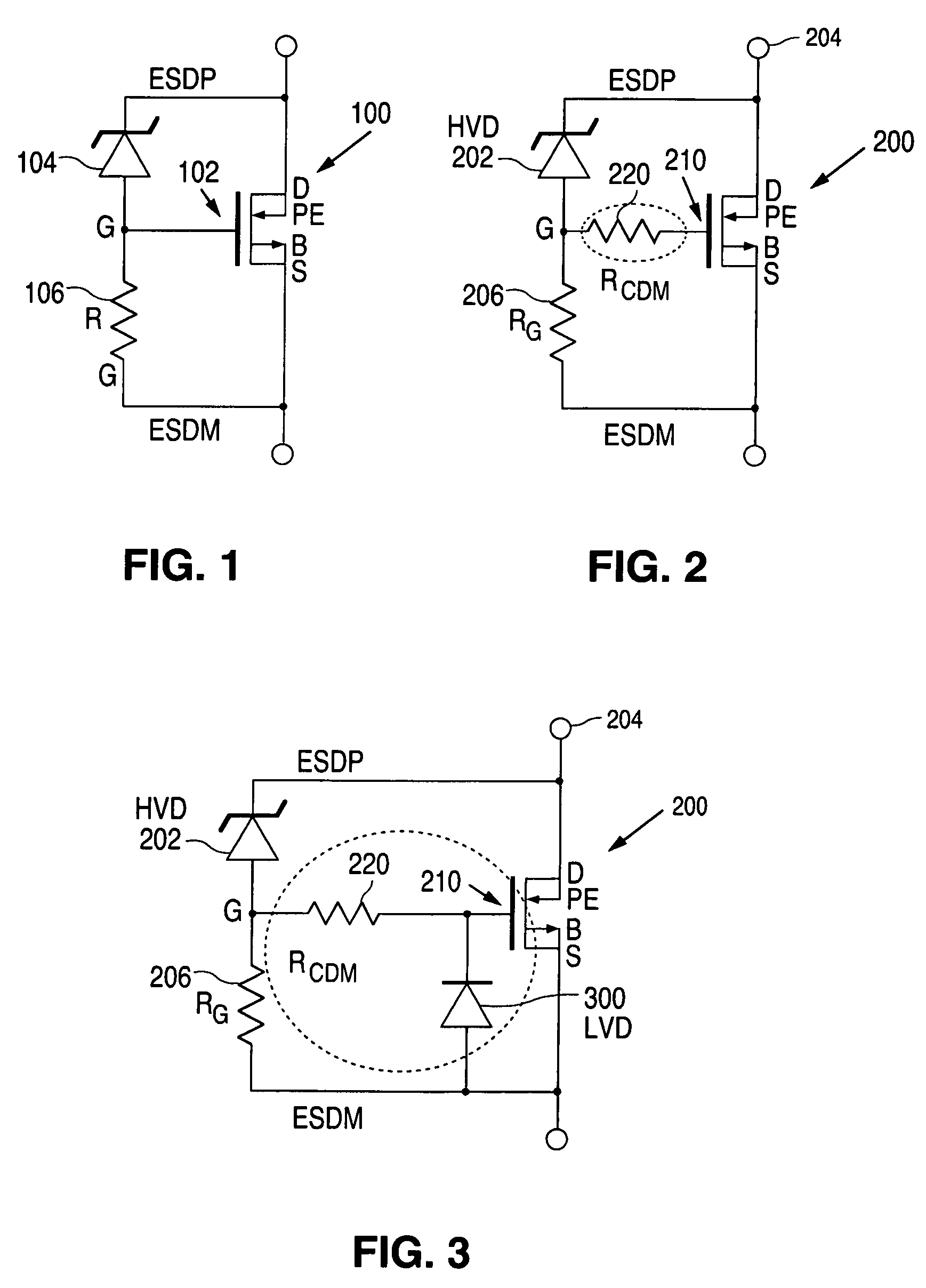
[0012]As mentioned above, high voltage ESD clamps operating with an avalanche diode reference have a high incidence of CDM failures when protecting pins with low internal loads. Failure analysis has shown gate-source region oxide damage, which suggests that the failure mechanism is gate-source breakdown in CDM pulse time domain. The dominant current path is related to the high side avalanche diode capacitance.

[0013]In particular, comparisons of the TLP and the very fast TLP (vfTLP) show significant differences in the clamping voltage due to the difference in the measurement time domain. Also, comparisons of vfTLP measurements made for clamps with and without a high side reference voltage component, show a three times higher gate current when a voltage reference component such as avalanche diode 202 is included.

[0014]The present invention therefore seeks, in particular, to address the high failure rates for ESD clamps with high side reference voltage under vfTLP conditions, especiall...


PUM

PropertyMeasurementUnit
timeaaaaaaaaaa
gate voltageaaaaaaaaaa
voltageaaaaaaaaaa

Abstract

In a high voltage ESD protection structure with a gate voltage reference and low impedance load, the CDM robustness of the structure is improved by including a gate resistor and a reverse path diode.

Description

FIELD OF THE INVENTION[0001]The invention relates to Electrostatic Discharge (ESD) protection. In particular it relates to protection against high speed pulses as defined by the charged device model (CDM).BACKGROUND OF THE INVENTION[0002]In order to control the turn-on of high voltage electrostatic discharge (ESD) protection clamps, the control gates of the clamps are commonly controlled using a voltage reference such as an avalanche diode connected between the high voltage pad and the control gate, as shown in FIG. 1, which shows an NLDMOS-SCR 100 with gate 102 connected to a voltage reference defined by avalanche diode 104 connected to the gate 102 and to ground via resistor 106.[0003]However, while these devices work well for relatively low frequency pulses such as the 100 ns human body model (HBM) pulses, this is not the case with very fast TLP (of the order of 2 ns), as defined by the charged device model (CDM) pulse. In the case of CDM pulses, these clamps demonstrate low pass...

Claims


Application Information

Patent Timeline
Patent Type & Authority Applications(United States)
IPC IPC(8): H01L27/06H01R43/00
CPCY10T29/49117H01L27/0262
Inventor VASHCHENKO, VLADISLAV
Owner NAT SEMICON CORP
Why Eureka
Try Eureka