
Semiconductor device, electric circuit using the same and method of controlling electric circuit

a technology of electric circuit and current detection device, which is applied in the direction of pulse generator, pulse technique, electronic switching, etc., can solve the problems of difficulty in monitoring the operation of hemt in an on-chip manner without an increase in power consumption, and electric power consumption in this current detection device. achieve the effect of not increasing the power consumption ra

Active Publication Date: 2012-03-08
SANKEN ELECTRIC CO LTD
View PDF6 Cites 7 Cited by
  • Summary
  • Abstract
  • Description
  • Claims
  • Application Information

AI Technical Summary

Benefits of technology

[0020]Thus, according to the present invention, the operation of a HEMT can be monitored on an on-chip basis without increasing the power consumption rate. Thus, an electric circuit can be operated optimally by using the configuration according to the present invention.

Problems solved by technology

However, when detecting an electric current by means of a current detection device, electric power is consumed in this current detection device in addition to the power consumed for the intrinsic operation of HEMT.
It has been difficult to monitor the operation of HEMT in an on-chip manner without an increase of power consumption.

Method used


Image

  • Semiconductor device, electric circuit using the same and method of controlling electric circuit
  • Semiconductor device, electric circuit using the same and method of controlling electric circuit
  • Semiconductor device, electric circuit using the same and method of controlling electric circuit

Examples


Embodiment Construction

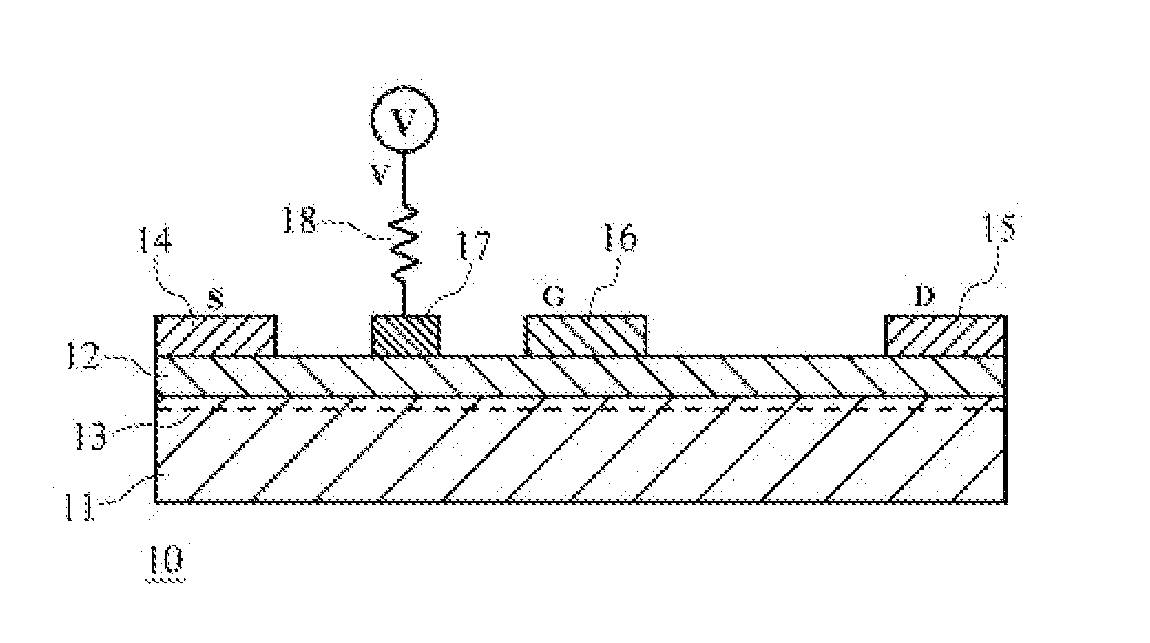
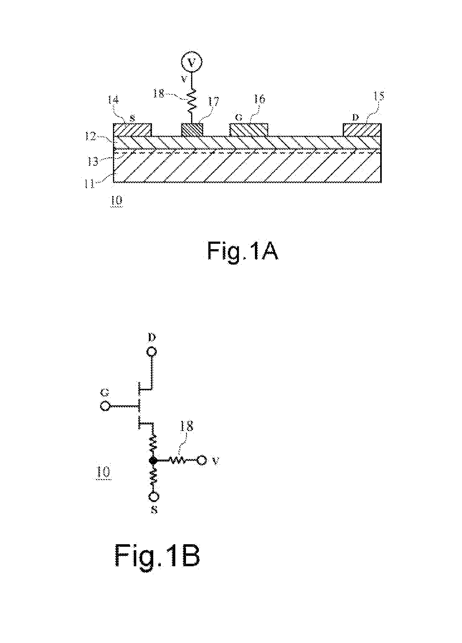
[0027]A semiconductor device according to the present invention can find preferable applications in the field of switching devices that operate with highpower. The semiconductor device is a so-called HEMT (high electron mobility transistor) in which a second semiconductor layer is formed on a first semiconductor layer and a channel of two-dimensional electron gas (2DEG) is formed along the hetero-junction interface of them and controlled for on and off by a voltage applied to the gate electrode of the semiconductor device. The operation of the device can be monitored particularly in terms of the potential between the main electrodes thereof.

[0028]FIG. 1A is a schematic cross-sectional view of the semiconductor device according to the present invention, illustrating the structure thereof. FIG. 1B is an equivalent circuit diagram of the device of FIG. 1A.

[0029]As seen from FIG. 1A, an electron supply layer 12, which is the second semiconductor layer, is formed on a channel layer 11, w...


PUM


Abstract

The operation of a HEMT is monitored on an on-chip basis without increasing the power consumption rate. In a semiconductor device 10, an electron supply layer 12 is formed on a channel layer 11. A two-dimensional electron gas (2DEG) layer 13 is formed at the side of the channel layer of the hetero-junction interface. Electrons flow through the 2DEG layer 13 between a source electrode 14 formed on the surface of the electron supply layer 12 and a drain electrode 15 that is formed on the same surface. A potential detection electrode 17 is arranged on the electron supply layer 12 between the gate electrode 16 and the source electrode 14. A resistor 18 having a sufficiently high resistance value makes the electric current flowing to the potential detection electrode 17 negligible relative to the drain current in operation.

Description

BACKGROUND OF THE INVENTION[0001]1. Field of the Invention[0002]The present invention relates to a semiconductor device designed to operate by using two-dimensional electron gas as channel, an electric circuit using such a semiconductor device and a method of controlling such an electric circuit.[0003]2. Description of the Related Art[0004]HEMT (high electron mobility transistor) is known as typical semiconductor device that employs two-dimensional electron gas (2DEG) as channel for operation. In a HEMT, 2DEG is formed along the interface of a channel layer (non-doped GaN, for example) and an electron supply layer (AlGaN, for example) at the side of the channel layer. A channel is formed in the 2DEG between the source and the drain of the transistor and turned on and off by the gate of the transistor for switching operations.[0005]Particularly, GaN-based HEMT, where GaN is a nitride semiconductor, is suited for switching operations for high power because the bandgap of GaN is large ...

Claims


Application Information

Patent Timeline
Patent Type & Authority Applications(United States)
IPC IPC(8): H03K17/06H01L23/544
CPCH01L27/0605H01L29/2003H01L29/7787H03K17/0822H01L2924/0002H01L2924/00
Inventor IWABUCHI, AKIOAOKI, HIRONORI
Owner SANKEN ELECTRIC CO LTD
Learn More