Power semiconductor module having sintered metal connections, preferably sintered silver connections, and production method

a technology of power semiconductor modules and metal connections, which is applied in the direction of semiconductor devices, semiconductor/solid-state device details, electrical apparatus, etc., can solve the problems of high production costs per item, large amount of waste heat induced by the needed high powers that have to be dissipated from the semiconductor elements, and only suited to relatively simple topologies. , to achieve the effect of increasing current carrying capacity and simplifying production

Inactive Publication Date: 2012-03-15
VINCOTECH HLDG R L
View PDF9 Cites 21 Cited by
  • Summary
  • Abstract
  • Description
  • Claims
  • Application Information

AI Technical Summary

Benefits of technology

[0011]Therefore, it is the object of the present invention to improve a power semiconductor module of the aforementioned type to the effect that the production is simplified, the heat dissipation as well as the electrical insulation are optimized and, at the same time, the current-carrying capacity is increased.

Problems solved by technology

In general, modern power modules involve the problem that significant quantities of waste heat induced by the needed high powers have to be dissipated from the semiconductor elements.
However, this solution involves the drawback that the production costs per item are relatively high.
Moreover, this arrangement is only suited for relatively simple topologies.
Finally, this known alternative exhibits a relatively great complexity and is less flexible than the arrangement of FIG. 4.
However, these prior solutions have the disadvantage that the thermal conditions are still unsatisfactory and that the constructional design with respect to the electrical insulation is relatively complicated.
Finally, the production of modules 600, 700 requires relatively expensive tools.

Method used


Image

  • Power semiconductor module having sintered metal connections, preferably sintered silver connections, and production method
  • Power semiconductor module having sintered metal connections, preferably sintered silver connections, and production method
  • Power semiconductor module having sintered metal connections, preferably sintered silver connections, and production method

Examples


Embodiment Construction

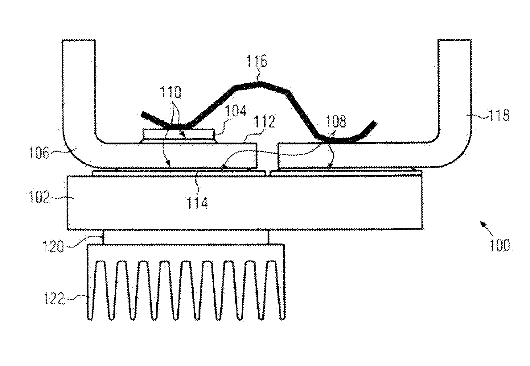
[0037]FIG. 1 shows in a schematic representation a first embodiment of a power semiconductor module 100 according to the present invention. The power semiconductor module 100, which will also be referred to as power module below, comprises a substrate 102 which is preferably made of ceramics. Of course, all other common circuit carrier materials may be used as well, e.g. high temperature resistant plastic materials or films.

[0038]A structured, printed and burnt-in silver layer 108 is provided on this substrate 102. This silver layer 108 serves the contact making with the inventive sintered silver connection 110. According to the present invention a power semiconductor device, which will also be referred to as chip below, is connected to a first lead frame element 106 on a first surface 112 by means of a sintered silver connection 110. The electrical contact with the substrate 102 is accomplished on the second surface, which is opposite the first surface 112, of the lead frame elemen...


PUM

PropertyMeasurementUnit
thicknessaaaaaaaaaa
thicknessaaaaaaaaaa
temperatureaaaaaaaaaa

Abstract

A power semiconductor module having a substrate (102), at least one power semiconductor device (104) and at least one lead frame element (106), and a method for producing such a power semiconductor module (100). The connection between the at least one first lead frame element and the power semiconductor device as well as the connection between the first lead frame element and the substrate comprise a sintered metal connection (110), preferably a sintered silver connection.

Description

BACKGROUND OF THE INVENTION[0001]The present invention relates to a power semiconductor module having a substrate, at least one power semiconductor device and at least one lead frame element. The present invention further relates to a production method for such a power semiconductor module.[0002]Specifically, the present invention relates to mounting and interconnection techniques for such power semiconductor modules, which will be referred to as “power modules” below. To this end, as is generally known, substantially two important electrical connections have to be closed, namely the connection between the semiconductor device (also referred to as “chip”) and a substrate as well as other internal devices on the one hand, and the electrical connection to the outer environment on the other hand.[0003]In general, modern power modules involve the problem that significant quantities of waste heat induced by the needed high powers have to be dissipated from the semiconductor elements. In ...

Claims


Application Information

Patent Timeline
Patent Type & Authority Applications(United States)
IPC IPC(8): H01L23/495H01L21/50
CPCH01L23/3735H01L23/49562H01L23/49811H01L24/29H01L24/32H01L24/33H01L24/48H01L24/73H01L24/83H01L25/072H01L2224/32245H01L2224/33181H01L2224/48137H01L2224/48227H01L2224/48247H01L2224/48472H01L2224/73265H01L2224/83191H01L2224/83192H01L2224/83193H01L2224/8384H01L2924/01013H01L2924/01029H01L2924/0103H01L2924/01047H01L2924/01049H01L2924/01073H01L2924/01079H01L2924/01082H01L2924/1815H01L2224/2919H01L2924/01005H01L2924/01019H01L2924/0102H01L2924/01023H01L2924/01024H01L2924/01033H01L2924/01044H01L2924/01045H01L2924/0105H01L2924/01074H01L2924/01076H01L2924/01077H01L2924/01078H01L2924/014H01L2924/0665H01L2224/48091H01L2224/29339H01L2924/00H01L2924/00014H01L2924/15787H01L2924/181H01L2924/00012H01L2224/45099H01L2224/45015H01L2924/207
Inventor SONTHEIMER, PETERORI, ATTILA
Owner VINCOTECH HLDG R L
Why Eureka
Try Eureka