Optical device and method of manufacturing the same

a technology of optical devices and manufacturing methods, applied in the field of optical techniques, can solve the problems of difficult forging of personal authentication media, difficult analysis of microstructures, and expensive manufacturing apparatus such as electron beam writers, and achieve the effect of high positional accuracy and stable formation of reflective layers

Inactive Publication Date: 2012-03-15
TOPPAN PRINTING CO LTD
View PDF4 Cites 57 Cited by
  • Summary
  • Abstract
  • Description
  • Claims
  • Application Information

AI Technical Summary

Benefits of technology

[0021]An object of the present invention is to provide an optical technique that m

Problems solved by technology

Securities, certificates, brands, media for personal authentication, etc. are required to be difficult to forge.
The microstructures are hard to analyze.
Further, in order to manufacture an optical device including the microstructure, an expensive manufacturing apparatus such as electron beam writer is necessary.
Simultaneously achieving a high producibility and a high positional accuracy is, however, impossible or very difficult.
For this reason, there is a possibility that the portion of the metal reflective layer corresponding to the “second region” has an excessively small thickness and thus has an i

Method used


Image

  • Optical device and method of manufacturing the same
  • Optical device and method of manufacturing the same
  • Optical device and method of manufacturing the same

Examples


example 1

Manufacture of Optical Device OD1

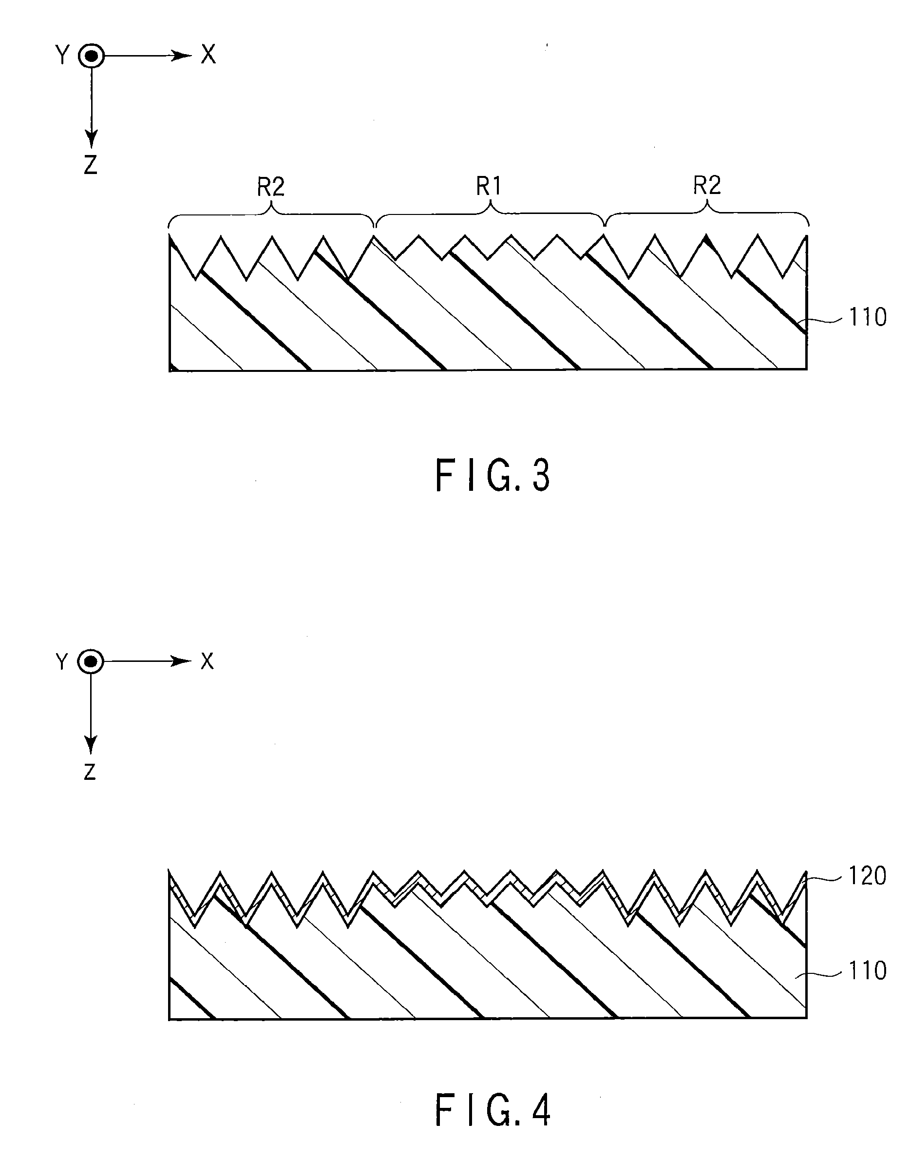
[0210]The above-described laminated body LB1 was subjected to an etching treatment. Specifically, the laminated body LB1 was exposed to 0.1 mol / L aqueous sodium hydroxide at 60° C. for 7 seconds. Thus, the portions of the reflective material layer 120 and the mask layer 130 corresponding to the second region R2 were removed.

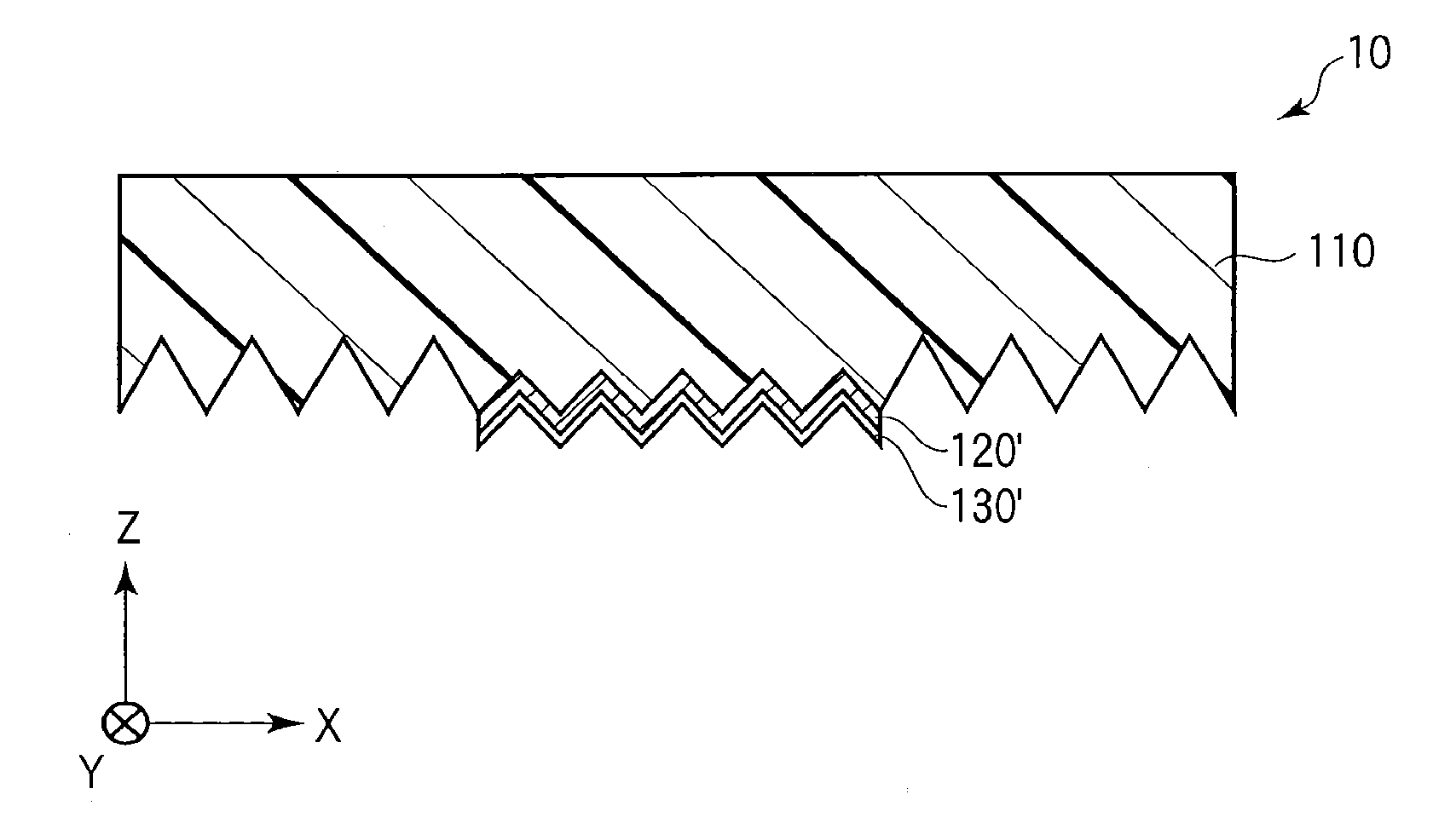
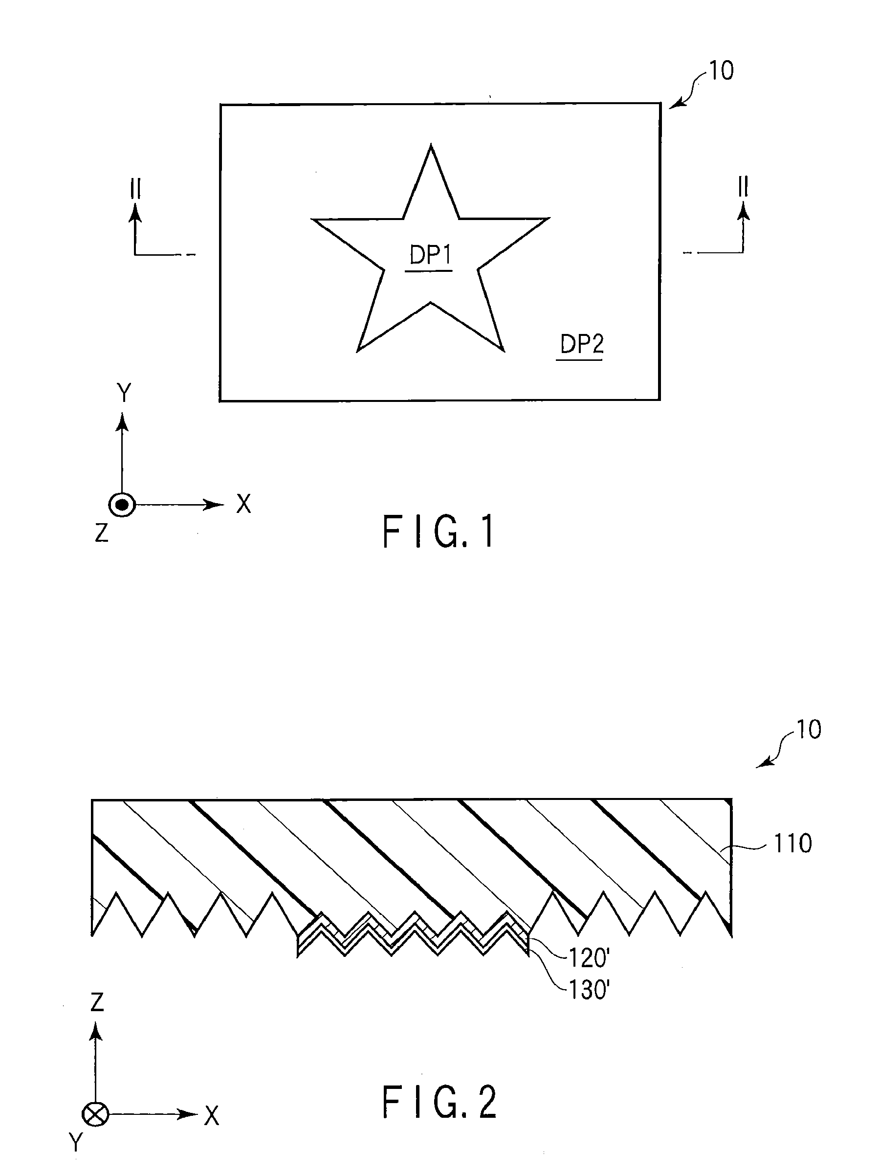
[0211]As above, the optical device 10 was manufactured. Hereinafter, the optical device 10 is referred to as an “optical device OD1”. The optical device OD1 had a laminated structure including the relief structure formation layer 110, the first layer 120′ covering only the entire first region R1 of the regions R1 and R2, and the second layer 130′ covering the entire first layer 120′.

[0212]In the optical device OD1, the mean thickness of the first layer 120′ was 50 nm. The mean diameter of the second layer 130′ was 20 nm.

example 2

Manufacture of Optical Device OD2

[0213]An optical device was manufactured by the same method as that for the optical device OD1 except that the minimum center-to-center distance of the recesses on the second region R2 was set at 200 nm, and the width of the opening and the depth of each recess were set at 200 nm and 160 nm, respectively. Hereinafter, the optical device is referred to as an “optical device OD2”.

[0214]In the optical device OD2, a ratio of the depth to the width of the opening of each groove on the first region R1 was 100 nm / 1,000 nm=0.1. A ratio of the depth to the width of the opening of each groove on the second region R2 was 160 nm / 200 nm=0.8.

[0215]In the optical device OD2, the mean thickness of the first layer 120′ was 50 nm. The mean diameter of the second layer 130′ was 20 nm.

example 3

Manufacture of Optical Device OD3

[0216]An optical device was manufactured by the same method as that for the optical device OD1 except that the pitch of the grooves on the first region R1 was set at 300 nm, the width of the opening and the depth of each groove were set at 300 nm and 100 nm, respectively, the minimum center-to-center distance of the recesses on the second region R2 was set at 375 nm, and the width of the opening and the depth of each recess were set at 375 nm and 300 nm, respectively. Hereinafter, the optical device is referred to as an “optical device OD3”.

[0217]In the optical device OD3, a ratio of the depth to the width of the opening of each groove on the first region R1 was 100 nm / 300 nm=0.33. A ratio of the depth to the width of the opening of each groove on the second region R2 was 300 nm / 375 nm=0.8.

[0218]In the optical device OD3, the mean thickness of the first layer 120′ was 50 nm. The mean diameter of the second layer 130′ was 20 nm.


PUM


Abstract

An optical device includes a relief structure formation layer, a first layer made of a first material having a refractive index different from that of a material of the relief structure formation layer, and a second layer made of a second material different from the first material and covering the first layer. A ratio of an amount of the second material at a position of the second region to an apparatus area of the second region is zero or smaller than a ratio of an amount of the second material at the position of the second sub-region to an apparatus area of the second sub-region.

Description

CROSS REFERENCE TO RELATED APPLICATIONS[0001]This application is a Continuation application of PCT Application No. PCT / JP2010 / 060306, filed Jun. 17, 2010 and based upon and claiming the benefit of priority from prior Japanese Patent Applications No. 2009-145532, filed Jun. 18, 2009; and No. 2010-092079, filed Apr. 13, 2010, the entire contents of all of which are incorporated herein by reference.BACKGROUND OF THE INVENTION[0002]1. Field of the Invention[0003]The present invention relates to an optical technique that offers, for example, forgery prevention effect, decorative effect and / or aesthetic effect.[0004]2. Description of the Related Art[0005]Securities, certificates, brands, media for personal authentication, etc. are required to be difficult to forge. Thus, in some cases, an optical device excellent in forgery prevention performance is provided on such articles.[0006]Most of the optical devices include a microstructure such as diffraction grating, hologram, lens array, etc. ...

Claims


Application Information

Patent Timeline
IPC IPC(8): B32B3/30B05D5/06
CPCB42D2033/18B42D2033/24G02B5/1842G02B5/32Y10T428/24612B42D25/29B42D25/324B42D25/328B05D5/063
Inventor YASHIKI, KAZUHIROSAWAMURA, CHIKARAUMEZAKI, KOJIKUBO, AKIRA
Owner TOPPAN PRINTING CO LTD
Why Eureka
Try Eureka