

Annealing thin films
- Summary
- Abstract
- Description
- Claims
- Application Information
AI Technical Summary
Benefits of technology
Method used
Image


Examples
Embodiment Construction
[0028]As noted, currently, copper indium gallium (di)selenide, also known as Cu2InGa(S, Se)4 or CIGS; and cadmium telluride (CdTe) are the major materials developed for use in thin film solar cells. With regard to the CIGS material, the prices of indium and gallium are high. Due to increasing demand in recent years for indium tin oxide (ITO) for use in flat panel displays, the price of indium continues to increase. With regard to CdTe, cadmium is toxic and tellurium is quite rare.
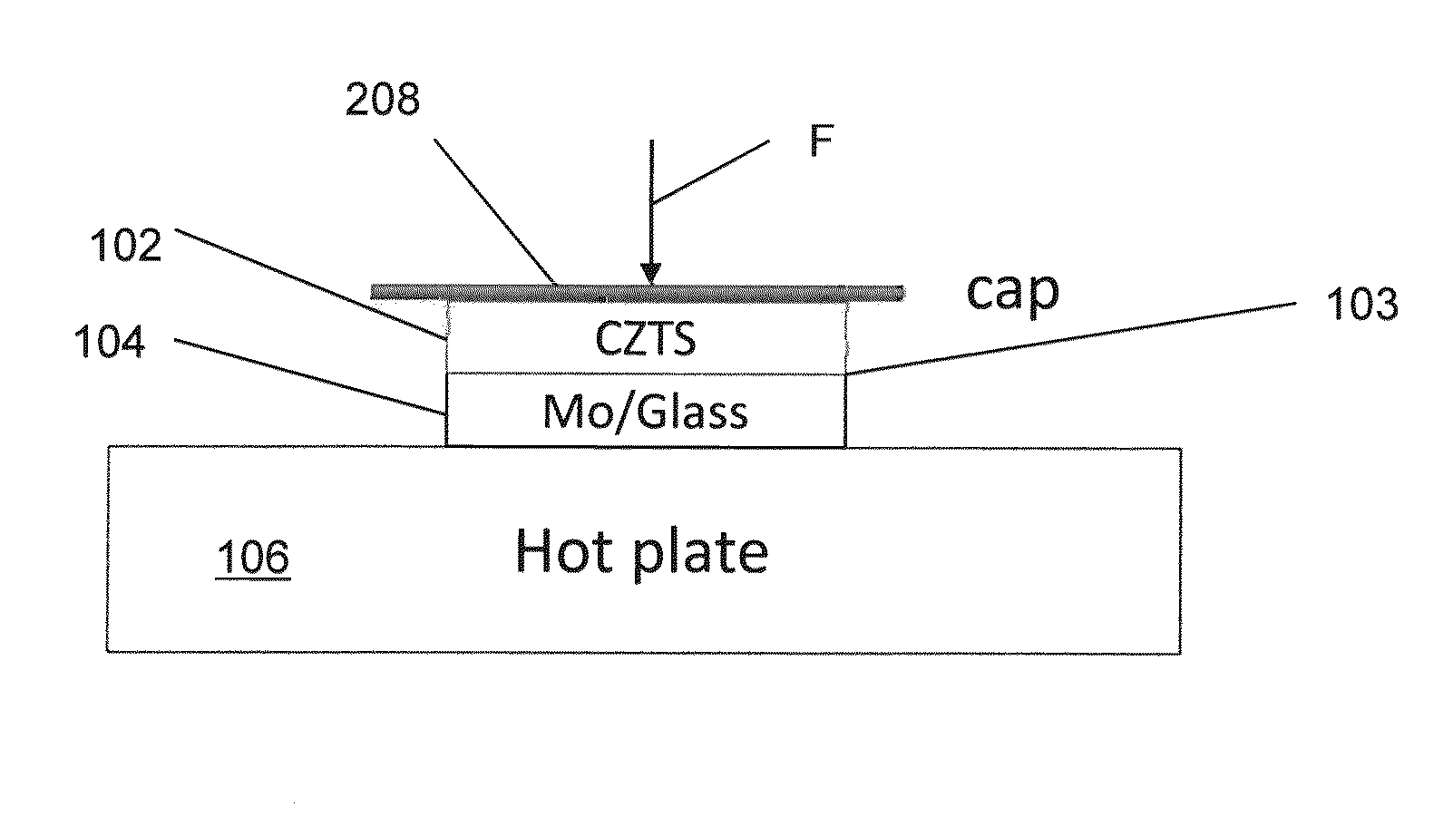
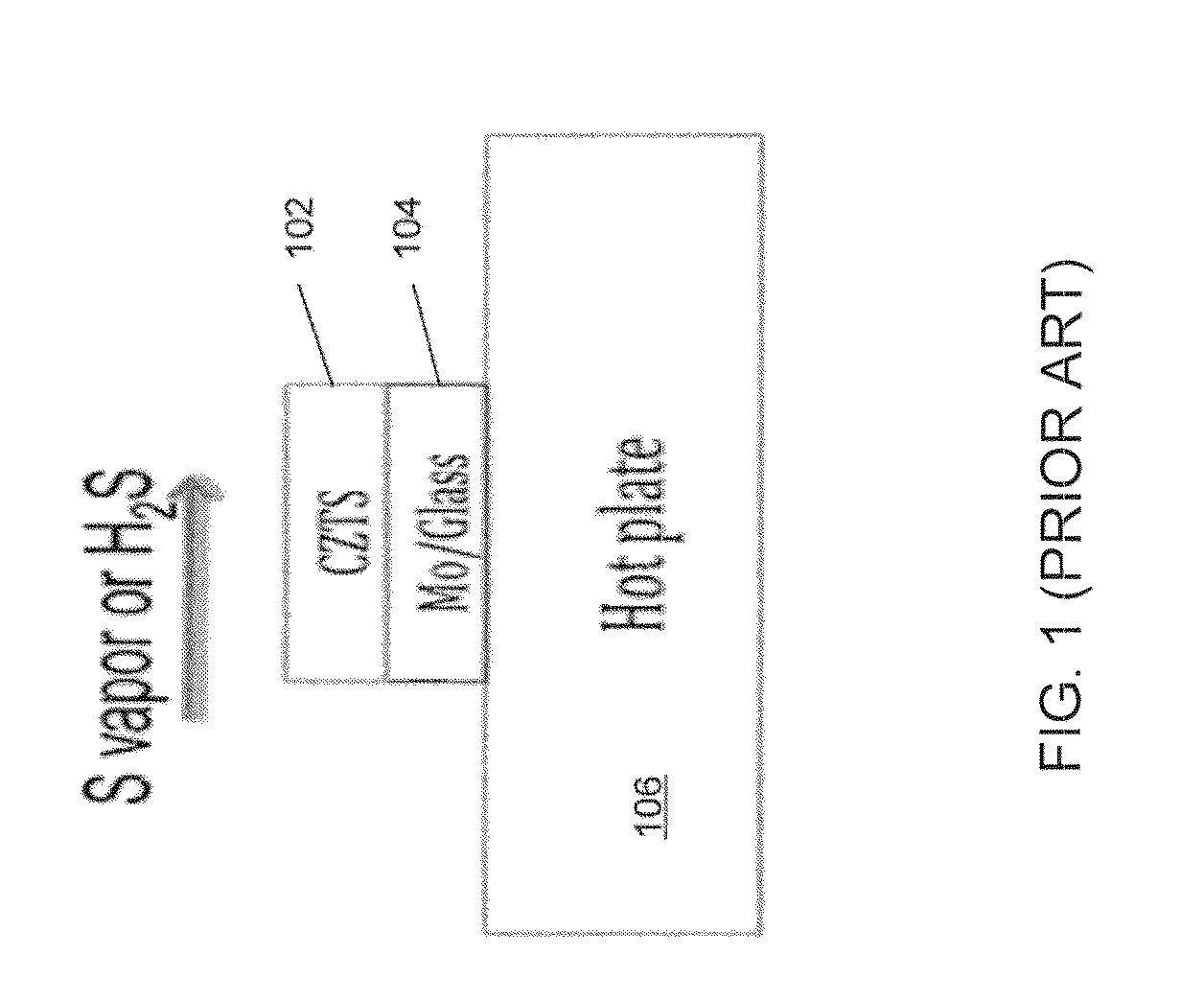
[0029]Kesterite, also known as Cu2ZnSnSxSe4-x or CZTS, holds the promise of low-cost, renewable solar cells, since all the elements used are cheap and earth-abundant. Costs may be lower, since CZTS is indium- and gallium-free; furthermore, less concern with toxicity is anticipated due to absence of cadmium and tellurium. CZTS films have been deposited by various techniques, including thermal evaporation, solution processes, electroplating, sputtering, and the like.
[0030]Most fabrication flows require high t...
PUM
 Abstract
Description
Claims
Application Information