Diode Having A Pocket Implant Blocked And Circuits And Methods Employing Same

a diode and pocket implant technology, applied in the direction of diodes, semiconductor/solid-state device details, diodes, etc., can solve the problems of large reliability problem of electrostatic discharge (esd), insufficient conduction for esd protection in soc technology, and relatively thin dielectrics susceptible to destructive breakdown and damage, etc., to achieve the effect of reducing the capacitance of the area junction

Active Publication Date: 2012-03-29
QUALCOMM INC
View PDF7 Cites 21 Cited by
  • Summary
  • Abstract
  • Description
  • Claims
  • Application Information

AI Technical Summary

Benefits of technology

[0010]A diode is offered. The diode includes a substrate and a first doped region doped with a first dopant. The first doped region is located in the substrate and does not have a pocket implant, thereby reducing area junction capacitance. The diode also includes a second doped region do

Problems solved by technology

Electro-static discharge (ESD) is a major reliability issue in integrated circuits (ICs).
These relatively thin dielectrics are susceptible to destructive breakdown and damage by excessive voltages from an ESD surge event.
Further, conventional diodes, such as the ESD surge diodes 20, 22 provided in FIG. 1, may not provide sufficient conduction for ESD protection in SOC technology.
Gated diodes can unacceptably decrease performance.
Increasing load capacitance can negatively affect protected circuits.
For example, increased load, capacitance can decrease switching times and frequency performance of a protected circuit, because charging time will be in

Method used


Image

  • Diode Having A Pocket Implant Blocked And Circuits And Methods Employing Same
  • Diode Having A Pocket Implant Blocked And Circuits And Methods Employing Same
  • Diode Having A Pocket Implant Blocked And Circuits And Methods Employing Same

Examples


Embodiment Construction

[0027]With reference now to the drawing figures, several exemplary embodiments of the present disclosure are described. The word “exemplary” is used herein to mean “serving as an example, instance, or illustration.” Any embodiment described herein as “exemplary” is not necessarily to be construed as preferred or advantageous over other embodiments.

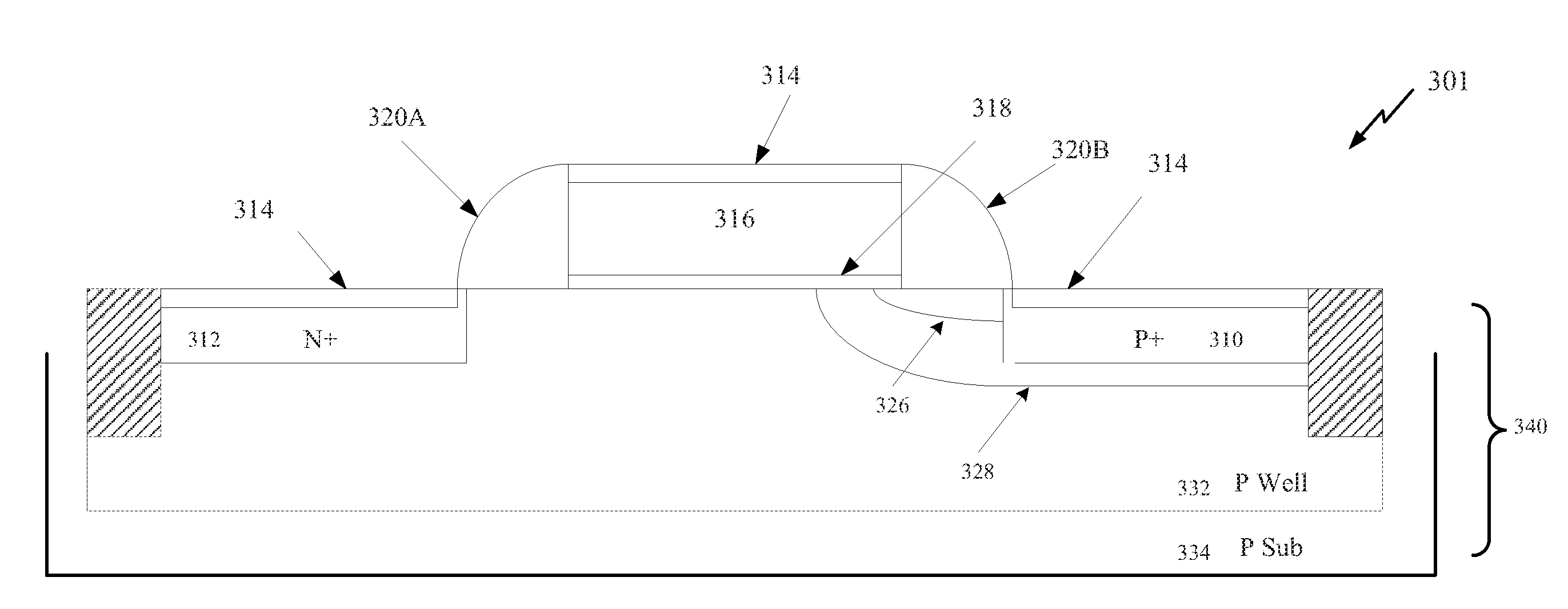
[0028]Aspects disclosed in the detailed description include examples of diodes, including gated diodes and shallow trench isolation (STI) diodes, exemplary methods of manufacture of the same, and related circuits and methods. The diode examples all have at least one halo or pocket implant blocked to reduce area capacitance. They may also feature at least one lightly-doped drain (LDD) implant blocked. In this manner, the diodes may be employed in circuits and other circuit applications having performance sensitive to such capacitance, but also seeking the performance characteristics of a gated or STI diode. Benefits of a gated diode include...


PUM


Abstract

Diodes, including gated diodes and shallow trench isolation (STI) diodes, manufacturing methods, and related circuits are provided without at least one halo or pocket implant thereby reducing capacitance of the diode. In this manner, the diode may be used in circuits and other devices having performance sensitive to load capacitance while still obtaining the performance characteristics of the diode. Such characteristics for a gated diode include fast turn-on times and high conductance, making the gated diodes well-suited for electro-static discharge (ESD) protection circuits as one example. Diodes include a semiconductor substrate having a well region and insulating layer thereupon. A gate electrode is formed over the insulating layer. Anode and cathode regions are provided in the well region. A P-N junction is formed. At least one pocket implant is blocked in the diode to reduce capacitance.

Description

CROSS REFERENCE TO RELATED APPLICATION[0001]This application is a continuation-in-part of U.S. patent application Ser. No. 12 / 403,418 filed Mar. 13, 2009, in the name of WORLEY, et al., the disclosure of which is expressly incorporated herein by reference in its entirety.TECHNICAL FIELD[0002]The technology of the present application relates to shallow trench isolation diodes and gated diodes and their use in circuits and related methods, including protection circuits, electro-static discharge (ESD) protection circuits, and high speed or switching circuitsBACKGROUND[0003]Electro-static discharge (ESD) is a major reliability issue in integrated circuits (ICs). ESD is a transient surge in voltage (negative or positive) that may induce a large current in a circuit. To protect circuits against damage from ESD surges, protection schemes attempt to provide a discharge path for both positive and negative ESD surges. Conventional diodes can be employed in ESD protection circuits to clamp the...

Claims


Application Information

Patent Timeline
IPC IPC(8): H01L23/62B05C11/00H01L21/762H01L29/78H01L29/861
CPCH01L27/0255H01L29/0649H01L29/6609H01L29/66356H01L29/7391H01L29/861H01L2924/0002H04B1/109H04B1/48H01L2924/00
Inventor JALILIZEINALI, REZAWORLEY, EUGENE R.SIANSURI, EVANDUNDIGAL, SREEKER
Owner QUALCOMM INC
Why Eureka
Try Eureka