
Semiconductor module design method and semiconductor module

a technology of semiconductor modules and semiconductor modules, applied in the direction of semiconductor devices, semiconductor/solid-state device details, instruments, etc., can solve the problems of high crystallinity, crystal defects found in the diameter of about 2 inches of such materials to a non-negligible extent, and give rise to degradation of high voltage characteristics. , to achieve the effect of low cost and high performance power

Inactive Publication Date: 2012-03-29
SANKEN ELECTRIC CO LTD
View PDF3 Cites 3 Cited by
  • Summary
  • Abstract
  • Description
  • Claims
  • Application Information

AI Technical Summary

Benefits of technology

[0012]In view of the above-identified problems, it is therefore an object of the present invention to provide a method of designing a semiconductor module that can dissolve the problems.
[0025]Thus, the present invention as described above can provide a semiconductor module loaded with high performance power semiconductor devices made from a compound semiconductor or made from diamond at low cost.

Problems solved by technology

However, while silicon is a material that allows crystal growth in a relatively easy manner and hence its crystallinity can be enhanced with ease, crystal growth is very difficult to such compound semiconductors and diamond and hence it is difficult to obtain a wafer showing a high degree of crystallinity.
For example, while a substantially defect-free silicon wafer having a diameter of 300 mm can be obtained on a commercial basis, crystal defects are found in a wafer of such a material having a diameter of about 2 inches to a non-negligible extent.
Of such crystal defects, those that are electrically active cause a leak current in a diode when the diode is reverse-biased to give rise to degradation of its high voltage characteristics.
For this reason, it is difficult for power semiconductor devices made from a compound semiconductor or diamond to perform to an expected degree.
Additionally, it is difficult to obtain high-performance power semiconductor devices made from such a material at low cost.
Thus, power semiconductor devices made from such a material are less popular than semiconductor devices made from silicon.
In short, it has been difficult to obtain a semiconductor module made from a compound semiconductor or diamond and loaded with high performance power semiconductor devices at low cost.

Method used


Image

  • Semiconductor module design method and semiconductor module
  • Semiconductor module design method and semiconductor module
  • Semiconductor module design method and semiconductor module

Examples


example

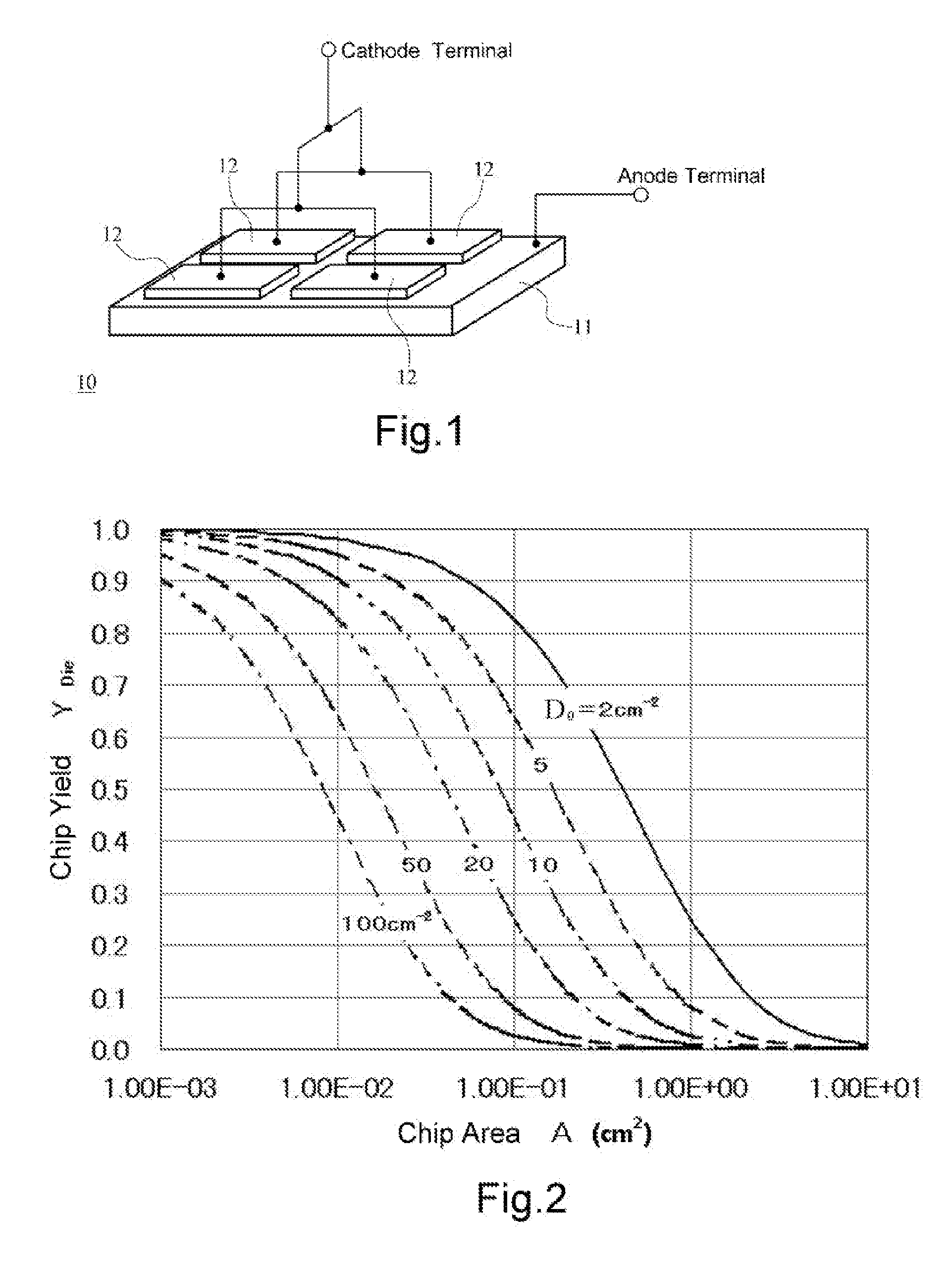
[0054]In an example, diodes were manufactured (for a semiconductor module) by using an SiC wafer whose D0 was 40 defects / cm2. The allowable current was about 50 A. The size of the diode chips was 2 mm square (X=200 μm). With this chip size (0.04 cm2), YDie=0.31 and RA=0.81. Thus, a value close to the peak value in the relationship between the index and the chip area A for D0=40 defects / cm2 was obtained. The yield of manufacturing semiconductor molecules (allowable current: 48 A), each having 6 diode chips of this size connected in series, was about 30%. FIG. 6A and FIG. 6B respectively show the forward bias characteristics and the reverse bias characteristics of the semiconductor modules. The yield of manufacturing semiconductor modules (allowable current: 50 A), each having a single diode chip with a sufficiently secured chip area, was about 2%, although they showed similar characteristics. While D0=40 defects / cm2 in this example, it will be clear that a higher yield can be achieve...


PUM


Abstract

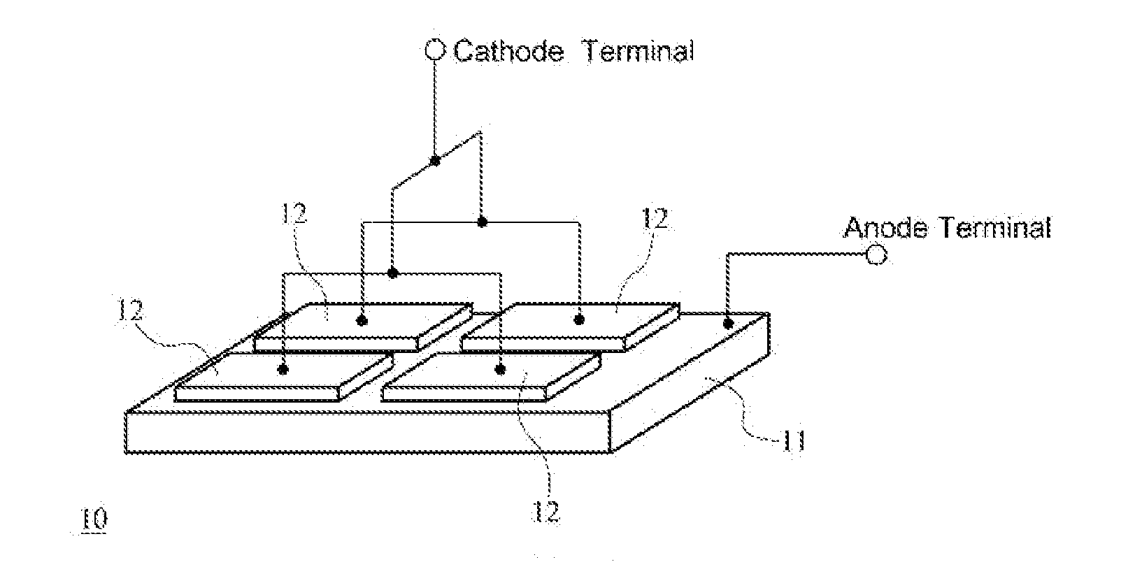
A semiconductor module made from a compound semiconductor or diamond and loaded with high performance power semiconductor devices can be obtained at low cost. In a semiconductor module, four (semiconductor chips) of same specifications are arranged in array, two longitudinally and two transversally, on a single lead frame. Achieving a high yield of manufacturing diode chips and reducing the unuseful area of diode chips need to be satisfied at the same time to obtain such a semiconductor module at low cost. The use of an index, which is the product of the yield YDie of manufacturing chips and the active region area ratio RA is effective for determining them. Thus, semiconductor modules can be obtained at a high yield by selecting a chip size that makes the index close to a peak value depending on the crystal defect density of a wafer to be used.

Description

BACKGROUND OF THE INVENTION[0001]1. Field of the Invention[0002]The present invention relates to a method of designing a semiconductor module loaded with a power semiconductor chip made from a compound semiconductor or the like. The present invention also relates to a semiconductor module obtained by using the method.[0003]2. Description of the Related Art[0004]Diodes and IGBTs (insulated gate bipolar transistors) made from silicon are being employed as power semiconductor devices designed to operate with a large electric current. A semiconductor chip loaded with such devices is then mounted on a lead frame or the like having a high heat dissipation effect. Such an assembly is formed by molding to produce a semiconductor module.[0005]A semiconductor module may be formed by mounting a plurality of semiconductor chips on a single lead frame. For example, Patent Document 1 (Jpn. Pat. Appln. Laid-Open Publication No. 2004-363339) describes a technique of mounting and arranging semicondu...

Claims


Application Information

Patent Timeline
Patent Type & Authority Applications(United States)
IPC IPC(8): G06F17/50
CPCH01L2924/10344H01L23/3107H01L23/49575H01L2224/32245H01L2924/10272H01L2924/1033H01L2924/12032H01L2924/1305H01L2924/13055H01L2924/12036H01L2924/00
Inventor KUMAKURA, HIROMICHIOGINO, HIROYUKIFUJIMOTO, KENJIUENO, MASANORI
Owner SANKEN ELECTRIC CO LTD
Learn More