Dual port static random access memory cell layout

a static random access and memory cell technology, applied in the field of semiconductor devices, can solve the problems of increased parasitic interconnection capacitance, adversely affecting read and write margins, and increasing parasitic interconnection capacitan

Active Publication Date: 2012-04-12
VLSI TECH LLC
View PDF1 Cites 25 Cited by
  • Summary
  • Abstract
  • Description
  • Claims
  • Application Information

AI Technical Summary

Problems solved by technology

However, simply adding two additional access transistors to create a dual port cell from a single port design may create issues that become more severe with smaller feature sizes and lower power supply voltages.
For example, the additional access transistors PG1 and PG4 may have a significant systematic mismatch due to asymmetry with access transistors PG2 and PG3 causing the access transistors PG1 and PG 4 t

Method used


Image

  • Dual port static random access memory cell layout
  • Dual port static random access memory cell layout
  • Dual port static random access memory cell layout

Examples


Embodiment Construction

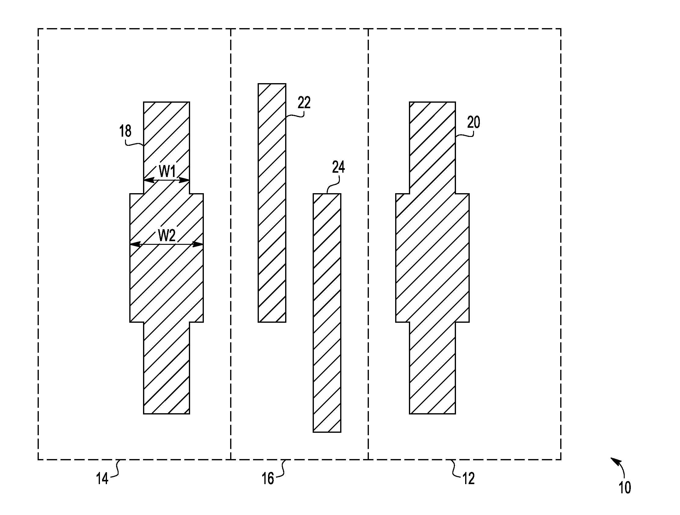
[0011]Generally, there is provided, an SRAM cell layout having symmetrical access transistors and multiple parallel-connected pull-down transistors. The symmetrical access transistors provide lower mismatch while the parallel-connected pull-down transistors provide a better width transition than one very wide transistor. Also, all of the access transistors are connected to the internal storage nodes using metal and are fully symmetrical, thus reducing mismatch. The layout also provides a better height to width ratio reducing the word line parasitic capacitance as compared to the prior art layout of FIG. 2.

[0012]In one aspect, there is provided dual port static random access memory cell having pull-down transistors, pull-up transistors, and pass transistors, comprising: a first active region having a first pull-down transistor coupled to a first data node, a second pull-down transistor coupled to a complementary data node that is complementary to the first data node; a first pass tra...


PUM


Abstract

A dual port static random access memory cell has pull-down transistors, pull-up transistors, and pass transistors. A first active region has a first pull-down transistor coupled to a true data node, a second pull-down transistor coupled to a complementary data node; a first pass transistor coupled to the true data node, and a second pass transistor coupled to the complementary data node. A second active region has the same size and shape as the first active region and has a third pull-down transistor coupled in parallel to the first-pull down transistor, a fourth pull-down transistor coupled in parallel to the second pull-down transistor; a third pass transistor coupled to the true data node, and a fourth pass transistor coupled to the complementary data node. A first pull-up transistor and a second pull-up transistor are located between the first and second active regions.

Description

BACKGROUND[0001]1. Field[0002]This disclosure relates generally to semiconductor memories, and more specifically, to a layout for a dual port static random access memory (SRAM) cell.[0003]2. Related Art[0004]Static random access memories are generally used in applications requiring high speed. A dual port SRAM may include more than one word line and / or more than one pairs of bit lines. FIG. 1 illustrates a schematic diagram of a prior art dual port SRAM cell having access transistors, or pass gates PG1-PG4, pull-up transistors PU1 and PU2, and pull-down transistors PD1-PD4. The SRAM cell of FIG. 1 is based on a conventional six transistor single port SRAM cell except that the SRAM cell of FIG. 1 has two parallel-connected pull-down transistors coupled to each storage node N1 and N2 instead of one very wide transistor, and two word lines. The pull-up and pull-down transistors are coupled to form two cross-coupled inverters with the connections of input and output terminals of the inv...

Claims


Application Information

Patent Timeline
IPC IPC(8): H01L21/70H01L21/8244
CPCH01L27/11H01L27/1104H01L29/4238Y10S257/903G11C11/412G11C11/413G11C8/16H10B10/00H10B10/12
Inventor MALINGE, PIERREHIGMAN, JACK M.PARIHAR, SANJAY R.
Owner VLSI TECH LLC
Why Eureka
Try Eureka