Graphene device and method for manufacturing the same

a graphene device and semiconductor technology, applied in the field of graphene semiconductor devices, can solve the problems increasing the cost of the carrier mobility of the graphene or the speed of the device, and achieving the effect of increasing the on-off ratio of the graphene device, speeding up the device, and not reducing the mobility of the graphene material

Active Publication Date: 2012-04-26
INST OF MICROELECTRONICS CHINESE ACAD OF SCI
View PDF9 Cites 7 Cited by
  • Summary
  • Abstract
  • Description
  • Claims
  • Application Information

AI Technical Summary

Benefits of technology

[0008]Using the device structure according to the invention, semiconductor doped regions are formed in contact with the graphene layer in the two regions neighouring the gate region on two opposite sides, through which the on-off ratio of the graphene device is increased without increasing the band gap of graphene, and thus the mobility of a graphene material, i.e., the speed of the device, will not be decreased, thereby increasing the applicability of the graphene material in CMOS devices.

Problems solved by technology

Although the graphene material shows many excellent physical properties, its application in a CMOS device as a channel material with high carrier mobility is confronted with many challenges.
Currently, some studies show that the on-off ratio of a graphene device may be increased to some extent by increasing the band gap of the graphene, but at the same time at the cost of the carrier mobility of the graphene or the speed of the device.

Method used


Image

  • Graphene device and method for manufacturing the same
  • Graphene device and method for manufacturing the same
  • Graphene device and method for manufacturing the same

Examples


Embodiment Construction

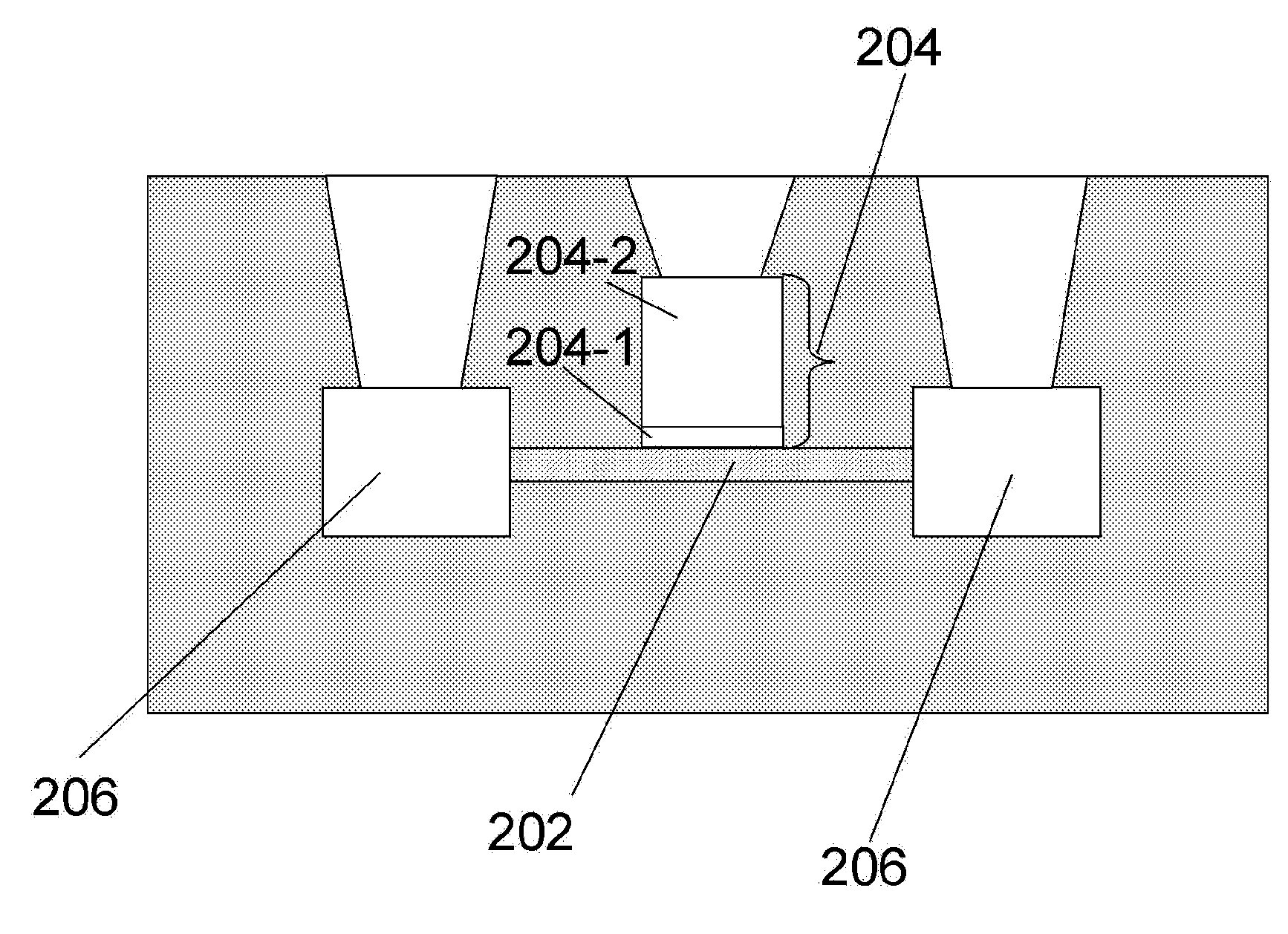
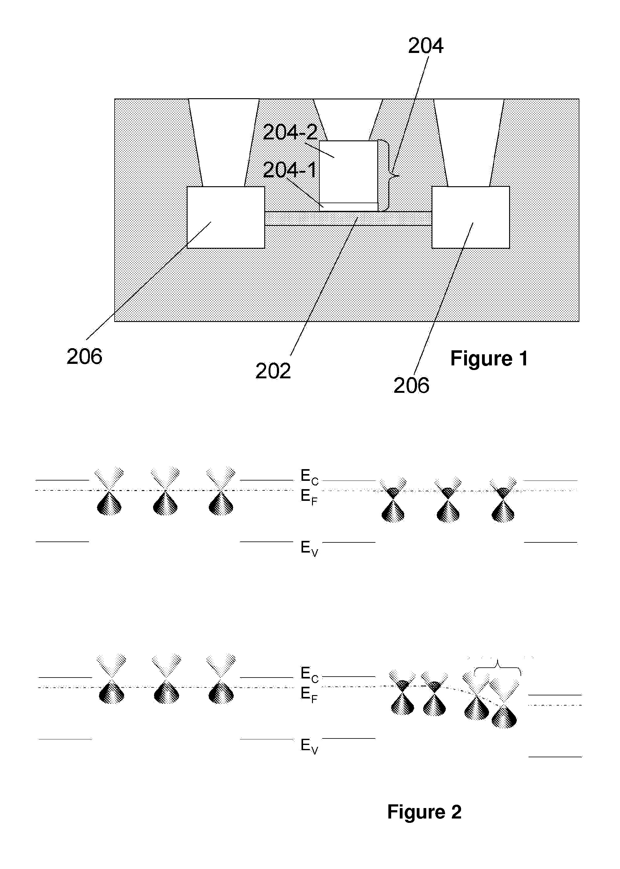
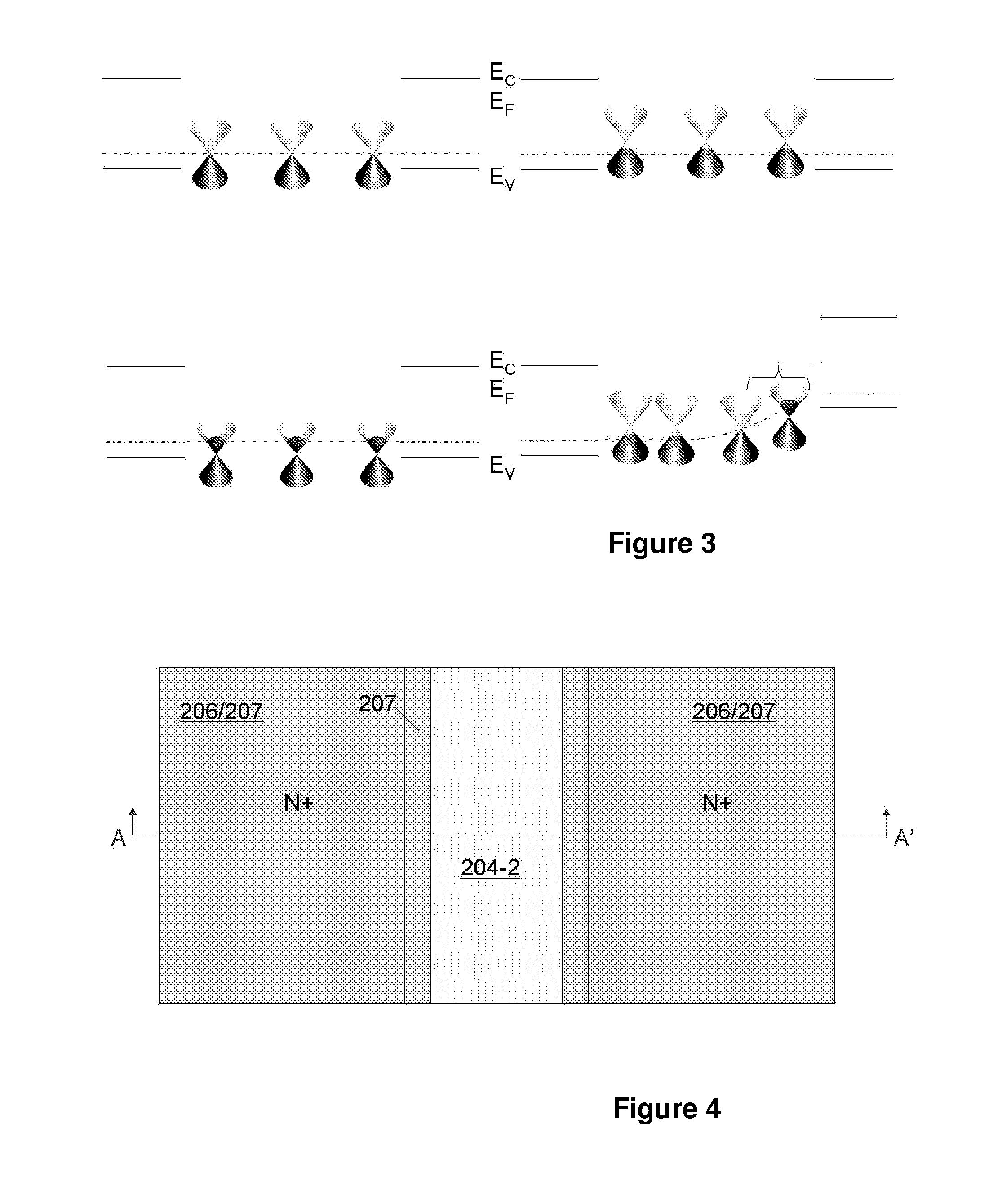
[0013]The invention in general relates to a graphene device and a manufacturing method thereof. The disclosure in the following provides many different embodiments or examples to implement various structure of the invention. For simplifying the disclosure of the invention, the components and arrangements of specific examples are described. Of course, they are just examples, and are not intended to limit the invention. Furthermore, the invention may repeat reference numerals and / or characters in various examples. Such a repeat is for the purpose of simplification and clarity, which is not indicative of the relationship between the various embodiments and / or arrangements under discussion. Furthermore, although the invention provides examples of various specific processes and materials, the applicability of other processes and / or the use of other materials will occur to those skilled in the art. In addition, a structure described in the following in which a first feature is “on” a seco...


PUM


Abstract

The invention provides a graphene device structure and a method for manufacturing the same, the device structure comprising a graphene layer; a gate region in contact with the graphene layer; semiconductor doped regions formed in the two opposite sides of the gate region and in contact with the graphene layer, wherein the semiconductor doped regions are isolated from the gate region; a contact formed on the gate region and contacts formed on the semiconductor doped regions. The on-off ratio of the graphene device is increased through the semiconductor doped regions without increasing the band gap of the graphene material, i.e., without affecting the mobility of the material or the speed of the device, thereby increasing the applicability of the graphene material in CMOS devices.

Description

CROSS-REFERENCE TO RELATED APPLICATIONS[0001]This application is a Section 371 National Stage Application of, and claims priority to, International Application No. PCT / CN2011 / 000291, filed on Feb. 24, 2011, which claimed priority to Chinese Application No. 201010287078.8, filed on Sep. 17, 2010. Both the international application and the Chinese application are incorporated herein by reference in their entireties.FIELD OF THE INVENTION[0002]The invention in general relates to a semiconductor device and a method for manufacturing the same, and in particular, to a graphene semiconductor device and a method for manufacturing the same.BACKGROUND OF THE INVENTION[0003]Currently, with respect to a prospective pilot study, what is most concerned about is whether a CMOS device still can be based on a silicon semiconductor substrate as it was after the technology generation of 11 nm to 16 nm. One research focus is to develop a new material system with higher carrier mobility and a new techni...

Claims


Application Information

Patent Timeline
Patent Type & Authority Applications(United States)
IPC IPC(8): H01L29/786H01L29/165H01L21/336B82Y40/00B82Y99/00
CPCH01L29/1606H01L29/778H01L29/78684H01L29/78618H01L29/78603
Inventor LIANG, QINGQINGJIN, ZHIWANG, WENWUZHONG, HUICAILIU, XINYUZHU, HUILONG
Owner INST OF MICROELECTRONICS CHINESE ACAD OF SCI
Why Eureka
Try Eureka