Organic thin film transistor having perpendicular channels in pixel structure and method for manufacturing same

a thin film transistor and perpendicular channel technology, applied in the field of display technology, can solve the problems of large power consumption and the highest driving voltage of the ips mode, and achieve the effects of reducing the size reducing the length of each channel, and increasing the on/off ratio of the tft devi

Inactive Publication Date: 2019-03-07
TCL CHINA STAR OPTOELECTRONICS TECH CO LTD
View PDF8 Cites 1 Cited by
  • Summary
  • Abstract
  • Description
  • Claims
  • Application Information

AI Technical Summary

Benefits of technology

[0019]In the organic thin film transistor having the perpendicular channels in the pixel structure and the method for manufacturing the same according to the present invention, advantages are that the thin film transistor (TFT) device has a plurality of channels with a perpendicular structure so as to reduce a length of each channel to increase on / off ratio of the TFT device, reduce the size of the TFT device, and improve the aperture ratio. An in-plane switching (IPS) pixel electrode is formed by a metallic material and applicable to a high resolution panel. The IPS pixel electrode is formed into a dimensional pixel electrode by etching the insulating layer, thereby not only to reduce a driving voltage, but also to increase a transmittance.

Problems solved by technology

The IPS mode has the highest driving voltage, and large power consumption.

Method used


Image

  • Organic thin film transistor having perpendicular channels in pixel structure and method for manufacturing same
  • Organic thin film transistor having perpendicular channels in pixel structure and method for manufacturing same

Examples


embodiments

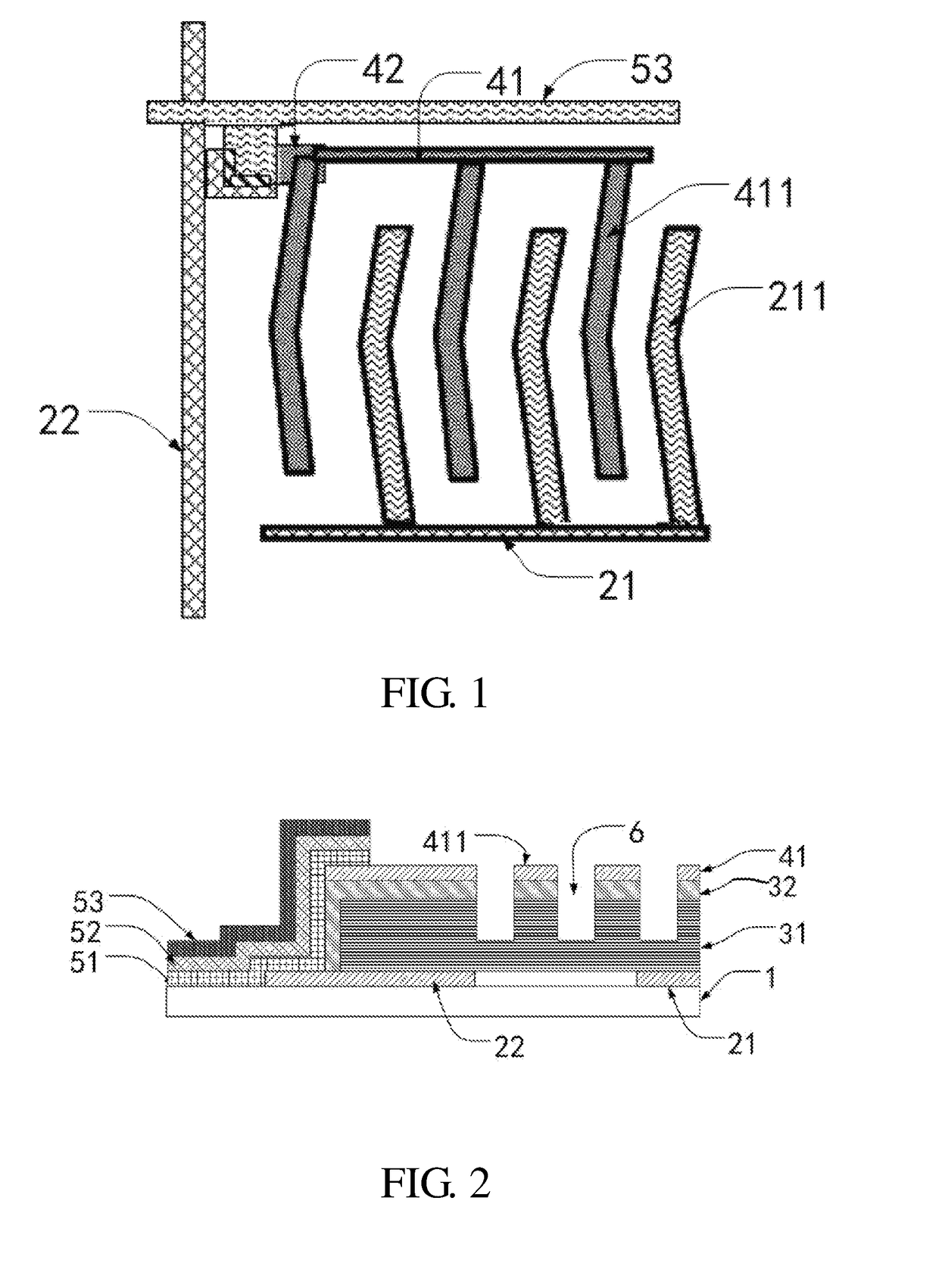
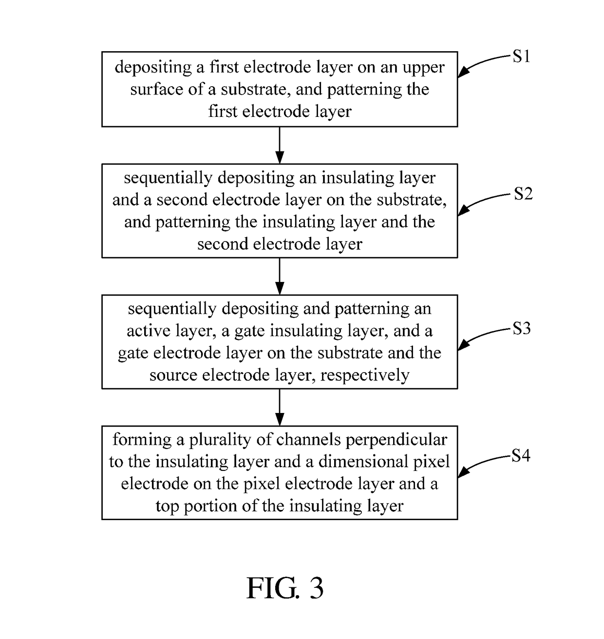
[0026]As shown in FIG. 1 and FIG. 2, an organic thin film transistor having a perpendicular channel in a pixel structure comprises a first electrode layer (a common electrode layer 21 and a source electrode layer 22), a second electrode layer (a pixel electrode layer 41 and a drain electrode layer 42), an insulating layer, an active layer 51, a gate insulating layer 52, and a gate electrode layer 53.

[0027]In this embodiment, the first electrode layer is distributed on a substrate 1. The first electrode layer comprises a common electrode area and a source electrode area. The common electrode layer 21 is distributed on the common electrode area, and the source electrode layer is distributed on the source electrode layer 22. After patterning, the common electrode layer 21 is divided into a plurality of common electrodes 211 separating from each other. The source electrode layer 22 forms a source electrode after patterning, and the source electrode connects with the common electrode lay...


PUM

PropertyMeasurementUnit
thicknessaaaaaaaaaa
thicknessaaaaaaaaaa
distanceaaaaaaaaaa

Abstract

An organic thin film transistor having perpendicular channels in a pixel structure is provided with a first electrode layer distributing on a substrate, and the first electrode layer having a source electrode layer; and a second electrode layer disposed on a top portion the substrate, and the second electrode layer having a pixel electrode layer and a drain electrode layer. An insulating layer is disposed between the first electrode layer and the substrate. A plurality of channels which are perpendicular to the insulating layer are distributing on the pixel electrode layer and the insulating layer. The channels divide the pixel electrode layer into a plurality of dimensional pixel electrodes separating from each other. An active layer is deposited on the drain electrode layer and the source electrode layer. A method for manufacturing the organic thin film transistor having the perpendicular channels in the pixel structure is also provided.

Description

CROSS-REFERENCE TO RELATED APPLICATIONS[0001]This is the U.S. National Stage of International Patent Application No. PCT / CN2017 / 109829, filed Nov. 8, 2017, which in turn claims the benefit of Chinese Patent Application No. 201710779318.8, filed Sep. 1, 2017.FIELD OF INVENTION[0002]The present invention relates to display technology, and specifically to an organic thin film transistor having perpendicular channels in a pixel structure and a method for manufacturing same.BACKGROUND OF INVENTION[0003]With development of display technologies, flat panel display devices, such as liquid crystal displays (LCDs), are widely used in mobile phones, televisions, personal digital assistants, digital cameras, laptops, desktop computers because of their advantages of high image quality, low power consumption, thin body, and wide application range. The LCD has become a mainstream in display devices.[0004]An organic light-emitting diode (OLED) display is known as an organic electroluminescent displ...

Claims


Application Information

Patent Timeline
Patent Type & Authority Applications(United States)
IPC IPC(8): G02F1/1368G02F1/1343
CPCG02F1/1368G02F1/134363G02F2201/40G02F2202/103H01L29/78642H01L29/7869G02F2001/134318G02F2201/124G02F2201/123G02F2202/022G02F1/13685H10K10/466G02F1/134318
Inventor LI, ZIRAN
Owner TCL CHINA STAR OPTOELECTRONICS TECH CO LTD
Why Eureka
Try Eureka