Germanium-based nmos device and method for fabricating the same

a nmos device and germanium-based technology, applied in the direction of semiconductor devices, basic electric elements, electrical equipment, etc., can solve the problem of rare dielectric materials which can meet the two requirements simultaneously, and achieve the effect of improving the on/off ratio of the device, reducing the sub-threshold slope, and small tunnelling resistan

Inactive Publication Date: 2013-03-21
PEKING UNIV
View PDF2 Cites 9 Cited by
  • Summary
  • Abstract
  • Description
  • Claims
  • Application Information

AI Technical Summary

Benefits of technology

[0021]By interposing two thin dielectric layers between the metal source / drain and the substrate, the Schottky barrier height between the source / drain and the channel formed through a contact can be effectively adjusted, an on / off ratio of the device is improved, and a sub-threshold slope is reduced. On one hand, as the bottom dielectric layer has a large pinning coefficient S, the Fermi level pinning effect can be inhibited so that a height of the Schottky barrier is varied as the work function of the metal varies. On the other hand, since the top dielectric layer has a small conduction band offset ΔEC, the electron wave function of the metal can be further blocked from introducing MIGS interface states into the semiconductor forbidden gap, and a small tunnelling resistance is ensured.
[0022]In order to effectively inhibit the Fermi level pinning effect, generally the bottom dielectric layer is required to have a pinning coefficient S, S>0.55, for example, a dielectric material having a high pinning coefficient S, such as silicon nitride (Si3N4), hafnium oxide (HfO2), hafnium silicon oxide (HfSiO4) or the like. Also, the top dielectric layer is required to have a conduction band offset ΔEC, ΔEC<1.0 eV, for example, a dielectric material having a low conduction band offset ΔEC, such as titanium oxide (TiO2), gallium oxide (Ga2O3), strontium titanium oxide (SrTiO3) or the like. According to the method, the Fermi level pinning effect can be alleviated, the electron barrier height can be lowered, and thus performance of the germanium-based Schottky NMOS device can be improved. Compared with a conventional single dielectric layer such as aluminium oxide (Al2O3) or the like, the Schottky barrier height can be lowered while low source / drain resistances can be maintained, and thus the performance of device can be substantially improved.

Problems solved by technology

However, a dielectric material which can meet the two requirements simultaneously is rare.

Method used


Image

  • Germanium-based nmos device and method for fabricating the same
  • Germanium-based nmos device and method for fabricating the same
  • Germanium-based nmos device and method for fabricating the same

Examples


Embodiment Construction

[0025]A detailed description of the invention will be described with reference to accompany drawings and detailed embodiments.

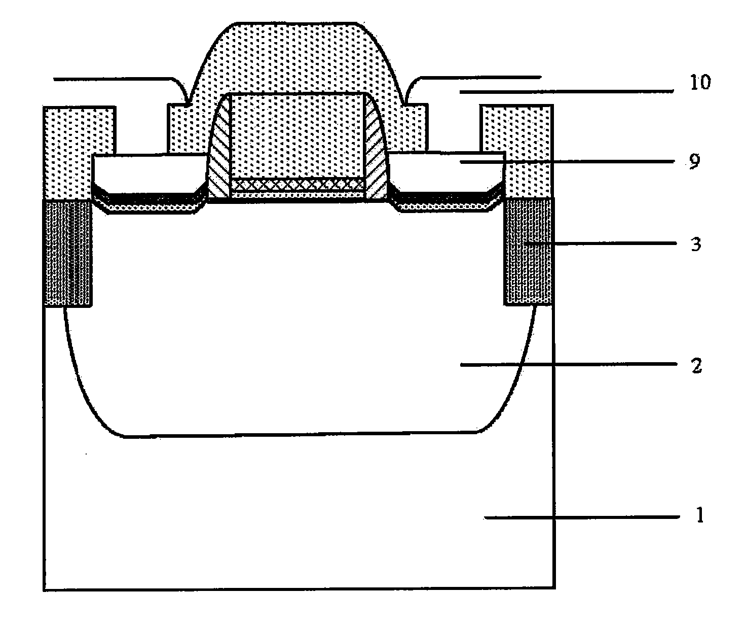
[0026]FIG. 1 shows a flow of a method for fabricating a germanium-based Schottky NMOS device according to a preferable embodiment. The method for fabricating the germanium-based Schottky NMOS device according to the embodiment of the invention includes the following steps.

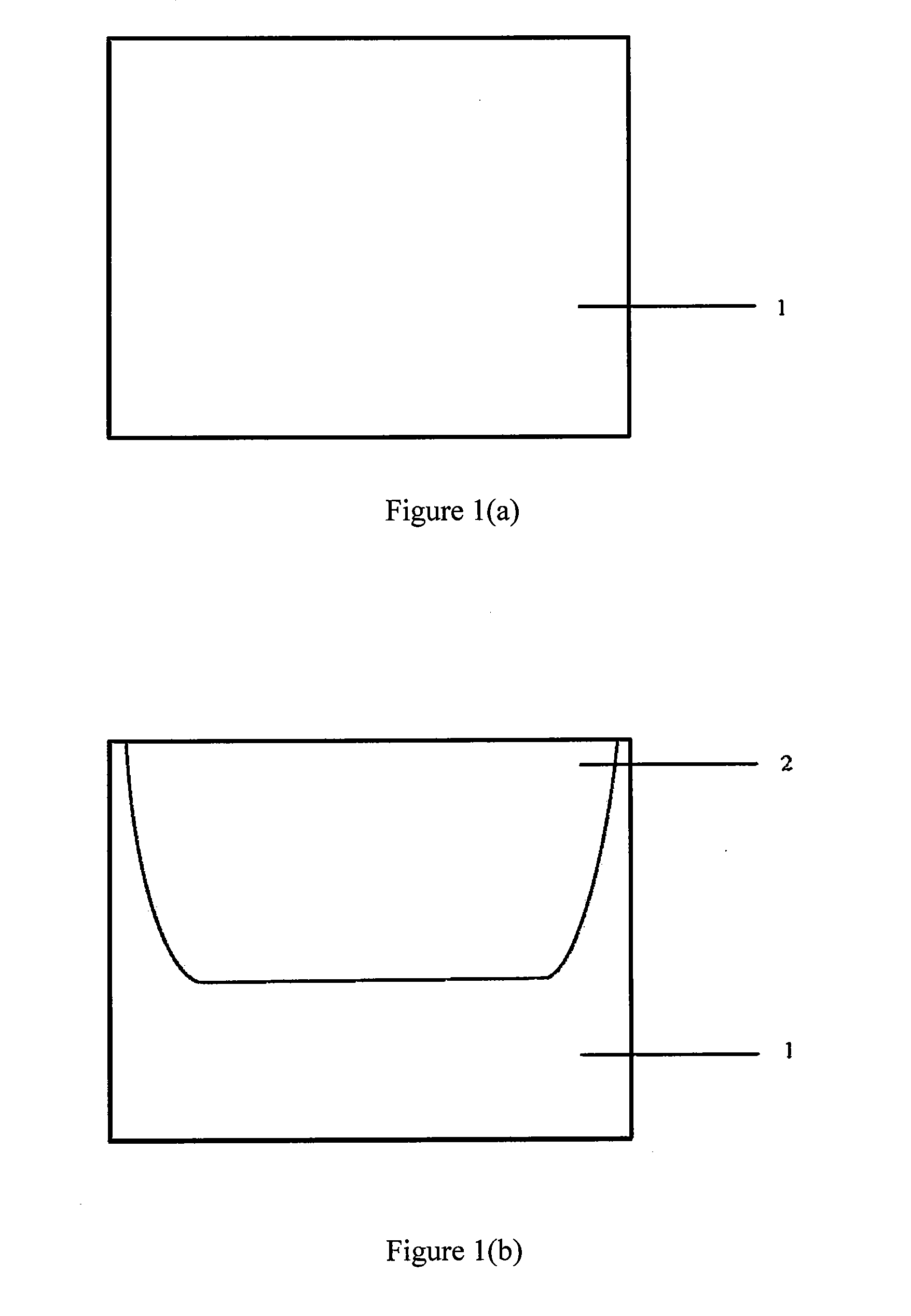
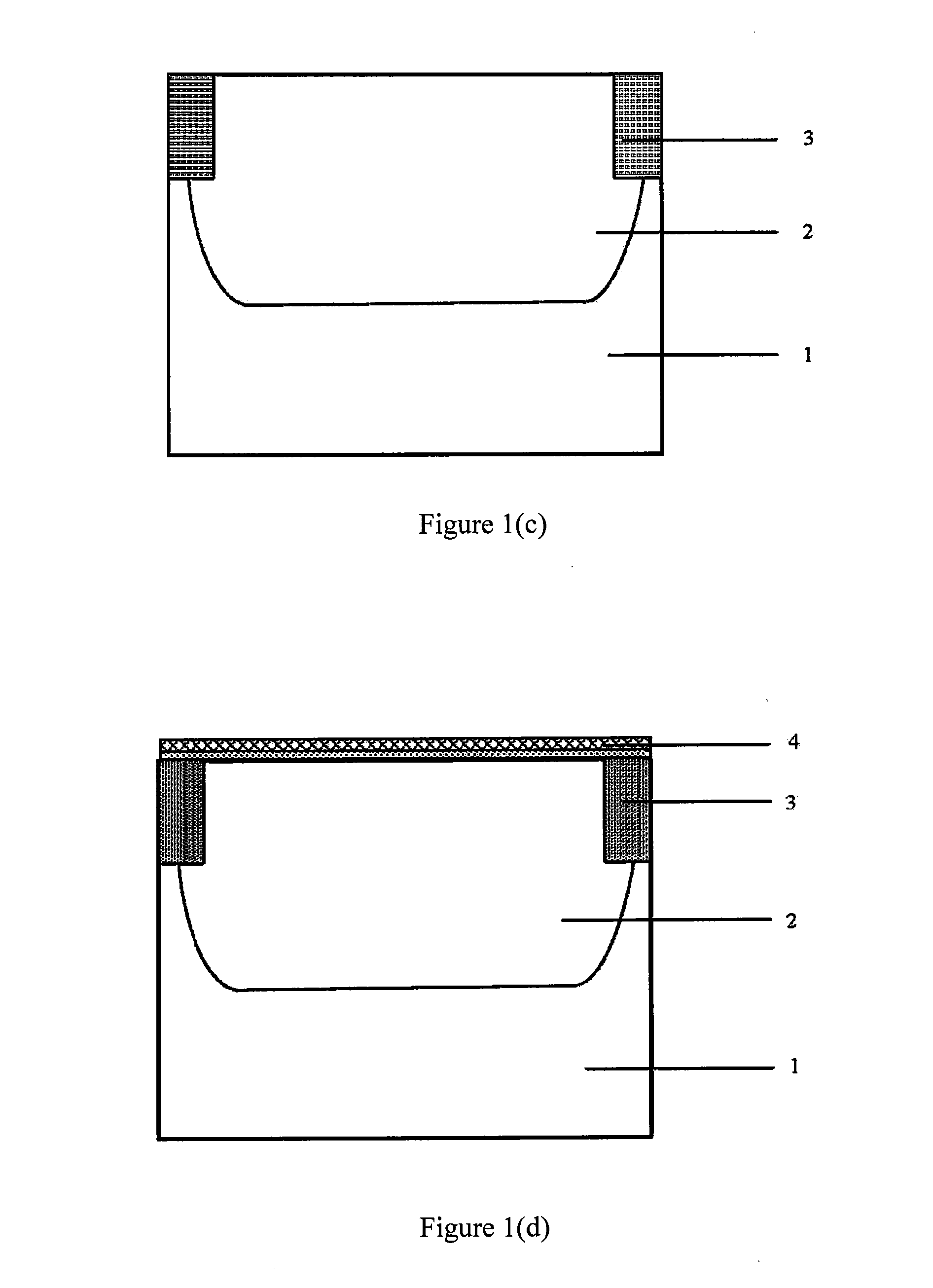
[0027]Step 1: A germanium-based substrate is provided. As shown in FIG. 1(a), an N-type semiconductor germanium substrate 1 is provided, wherein, a bulk germanium substrate, a germanium-on-insulator (GOI) substrate, an epitaxy germanium substrate or the like may be used as the semiconductor germanium substrate 1.

[0028]Step 2: A P-well region is fabricated. A silicon oxide layer and a silicon nitride layer are deposited over the semiconductor germanium substrate 1. A P-type well is defined by photolithograph process and the silicon nitride layer of the P-type well is removed by a reactive-ion...


PUM

PropertyMeasurementUnit
thicknessaaaaaaaaaa
thicknessaaaaaaaaaa
conduction band offset ΔECaaaaaaaaaa

Abstract

An embodiment of the invention provides a germanium-based NMOS device and a method for fabricating the same, which relates to fabrication process technology of an ultra-large-scale-integrated (ULSI) circuit. The germanium-based NMOS device has two dielectric layer interposed between a metal source/drain and a substrate. The bottom dielectric layer includes a dielectric material having a high pinning coefficient S such as hafnium oxide, silicon nitride, hafnium silicon oxide or the like, and the top dielectric layer includes a dielectric material having a low conduction band offset ΔEC such as titanium oxide, gallium oxide, strontium titanium oxide or the like. According to the method, Fermi level pinning effect can be alleviated, electron barrier height can be lowered, and thus performance of the germanium-based Schottky NMOS device can be improved. Compared with a conventional single dielectric layer such as aluminum oxide (Al2O3), Schottky barrier height can be lowered while low source/drain resistances can be maintained, and thus performance of the device can be significantly improved.

Description

CROSS-REFERENCES TO RELATED APPLICATION[0001]The present application claims priority to Chinese Patent Application No. 201110171004.2, filed on Jun. 23, 2011, which is incorporated herein by reference in its entirety as if set forth herein.FIELD OF THE INVENTION[0002]An embodiment of the invention relates to fabrication process technology of ultra-large-scale-integrated (ULSI) circuit, and particularly, to a germanium-based NMOS device and a method for fabricating the same.BACKGROUND OF THE INVENTION[0003]With the shrink of CMOS device, a traditional silicon-based MOS device has encountered many challenges, in which mobility degradation has become one of key limiting factors to further enhance the device performance. Compared with silicon, germanium has higher and more symmetrical low field carrier mobility. Furthermore, the fabrication process of germanium device is compatible with conventional CMOS process. Thus, the germanium-based device has become one of research hotspots.[0004...

Claims


Application Information

Patent Timeline
Patent Type & Authority Applications(United States)
IPC IPC(8): H01L29/78H01L21/283
CPCH01L29/78H01L29/41783H01L29/0895H01L29/66643H01L29/517
Inventor HUANG, RULI, ZHIQIANGAN, XIAGUO, YUEZHANG, XING
Owner PEKING UNIV
Why Eureka
Try Eureka