

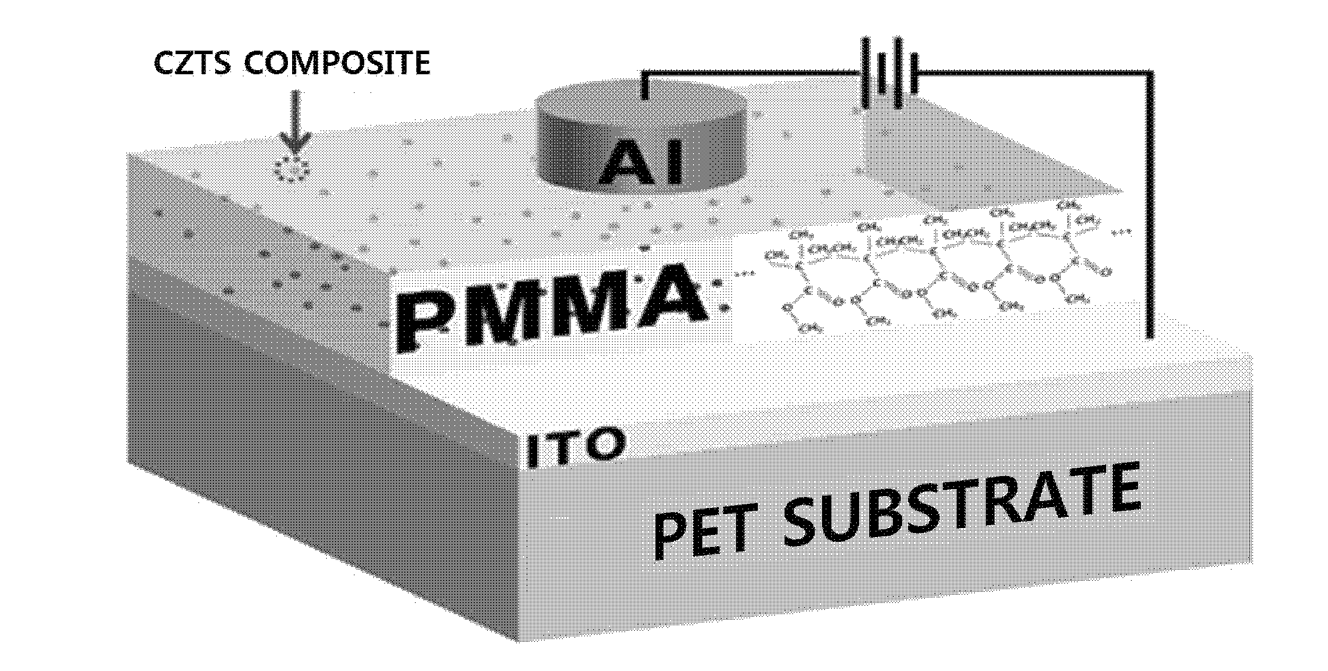
Nanocomposite-based non-volatile memory device and method for manufacturing same
a non-volatile memory and nanocomposite technology, applied in nanoinformatics, solid-state devices, instruments, etc., can solve the problem of not exceeding the size of the conductivity change of the organic memory device, and achieve the effect of reducing the sensing error, increasing the on/off ratio, and less noise in the circui
- Summary
- Abstract
- Description
- Claims
- Application Information
AI Technical Summary
Benefits of technology
Problems solved by technology
Method used
Image

Examples
examples
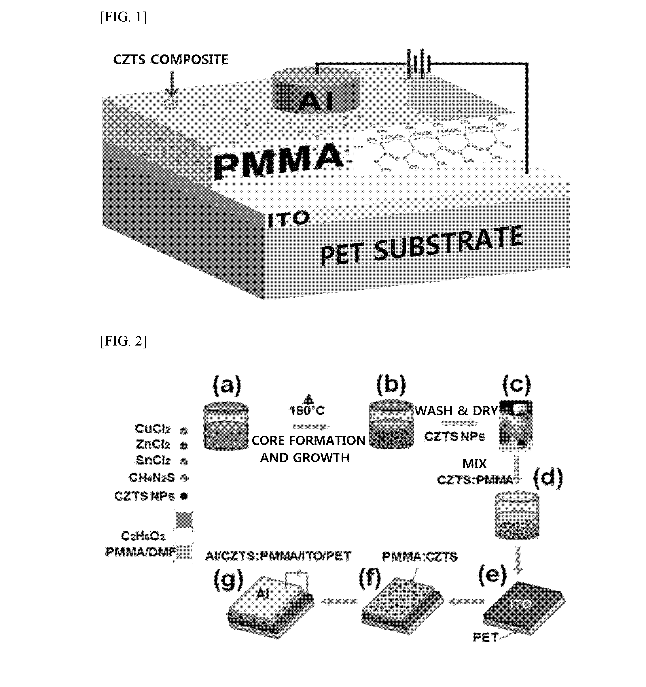
[0053]1. Synthesis of CZTS Nanocomposite
[0054](1) 2 mmol of copper(II)chloridedehydrate (CuCl22O), 1 mmol of zinc(II)chloride (ZnCl2), 1 mmol of tin(IV)chloridetetrahydrate (SnCl42O), and 8 mmol of thiourea (CH4N2S) were added to 40 ml of ethylene glycol and sufficiently mixed using a magnetic stirrer (FIG. 2(a)).
[0055](2) The mixed solution was put into a high pressure stainless steel container and sealed and then thermally treated at 180° C. for 6 hours (FIG. 2(b)).
[0056](3) After the thermally-treated solution was slowly cooled at room temperature, a by-product was rapidly separated using a centrifugal separator and then washed again with deionized water to remove. To remove other by-products generated during synthesis, the resultant product was washed with ethanol several times. Afterward, to completely remove the solvent, the resultant product was dried in a vacuum oven at 80° C., thereby obtaining a CZTS nanocomposite (FIG. 2(c)).
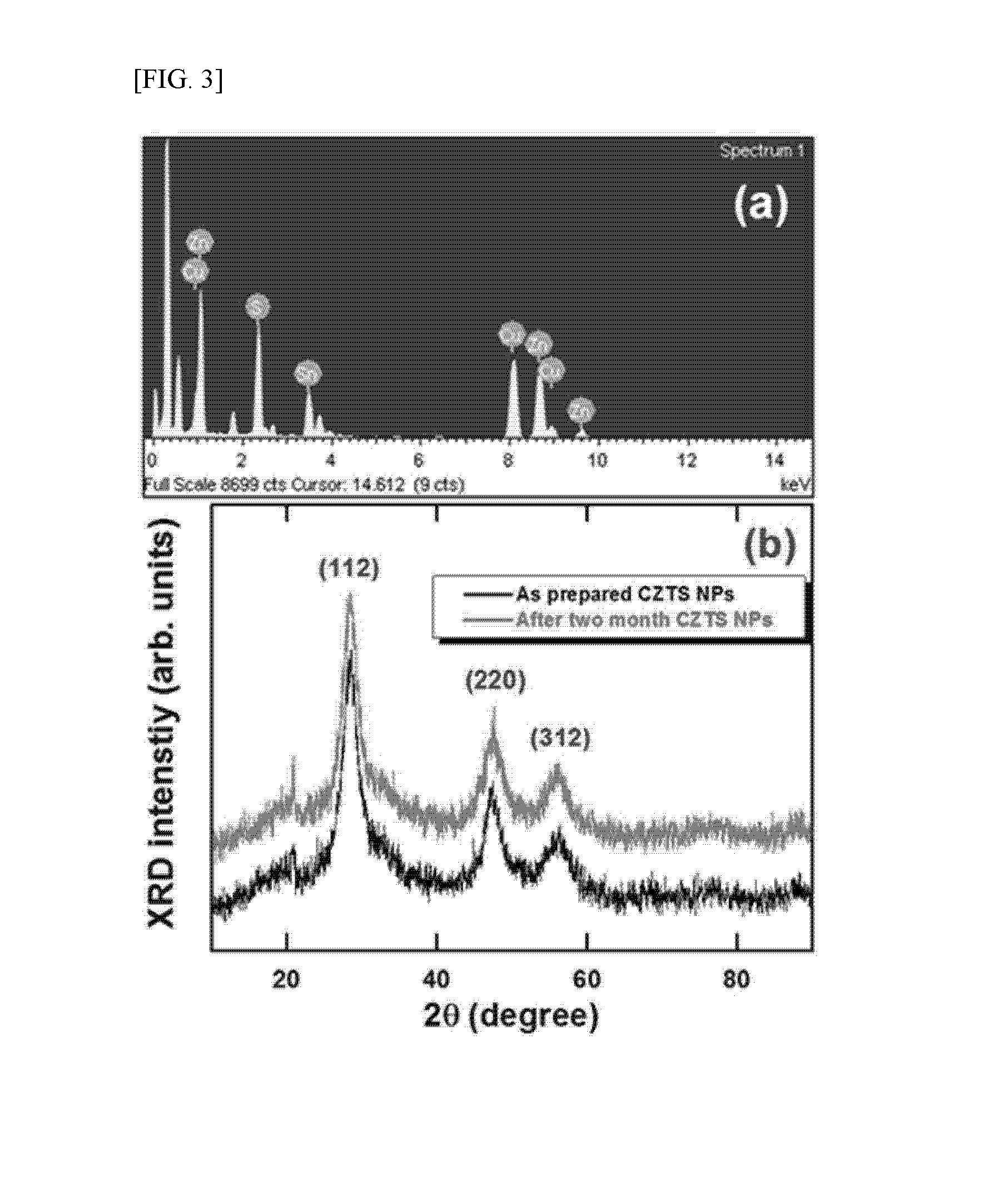
[0057](4) To identify components of the obtaine...
PUM
 Abstract
Description
Claims
Application Information