Wiring board
a wiring board and wiring technology, applied in the direction of electrical apparatus construction details, printed circuit non-printed electric components association, semiconductor/solid-state device details, etc., can solve the problems of common demand, difficulty in saving space in the wiring board, and simplifying the manufacturing process of the wiring board, so as to improve scalability, reduce the number of chip capacitors on the substrate, the effect of simplifying the manufacturing process
- Summary
- Abstract
- Description
- Claims
- Application Information
AI Technical Summary
Benefits of technology
Problems solved by technology
Method used
Image

Examples
first embodiment
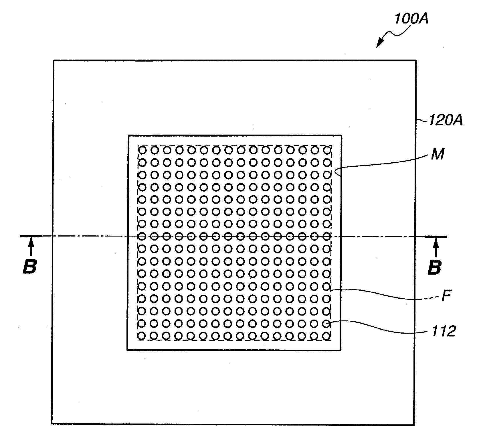
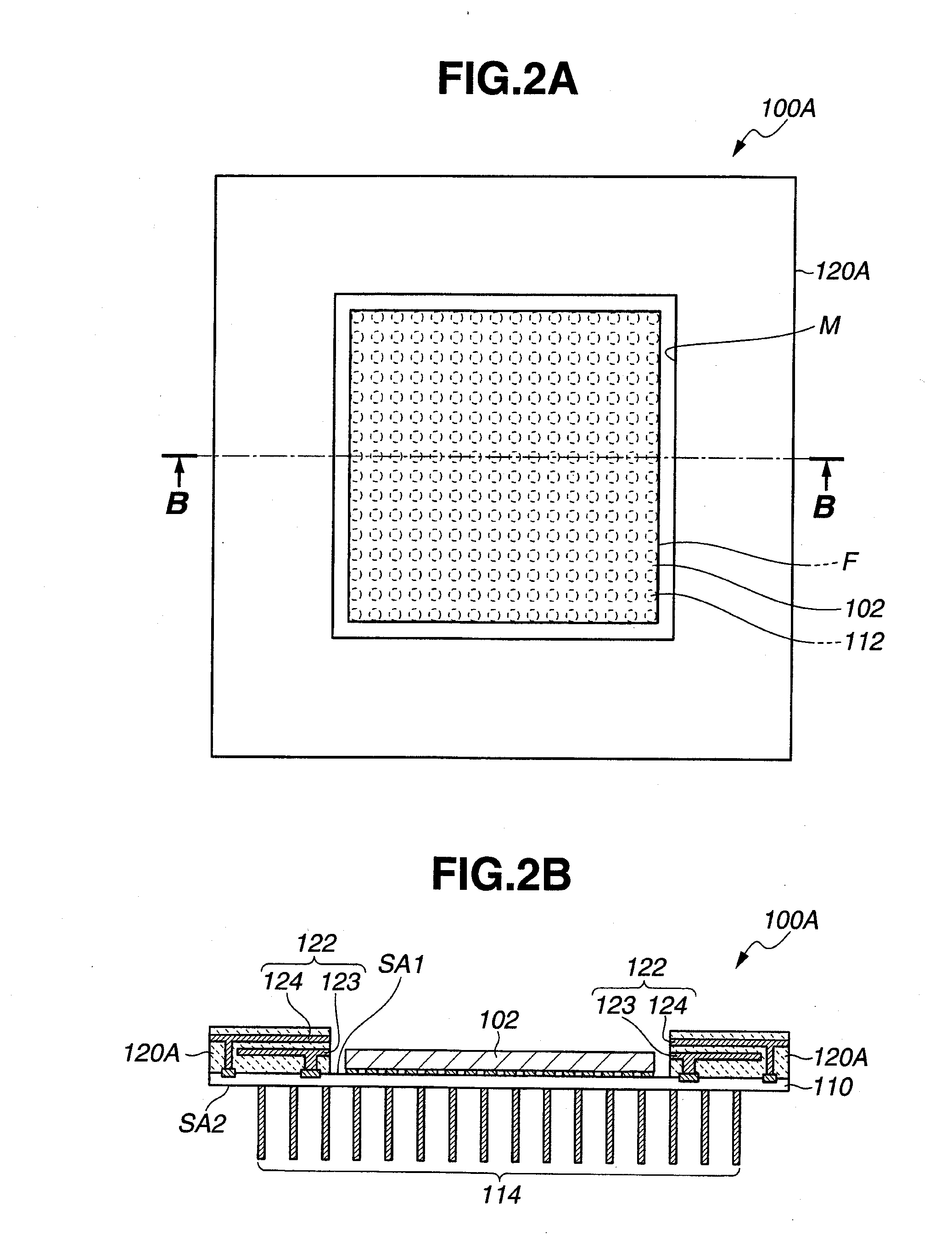
[0033]A wiring board 100A according to the first embodiment is designed to mount thereon a semiconductor chip 102 (as an electronic chip) and thereby function as a connector for connection of the semiconductor chip 102 to a printed circuit board of a computer etc. as shown in FIGS. 1A, 1B, 2A and 2B. The wiring board 100A includes a multilayer substrate 110 and a stiffener 120A (as a reinforcing member).
[0034]The multilayer substrate 110 is formed into a substantially square shape with first and second opposed main substrate surfaces SA1 and SA2. A chip mounting area F to which the semiconductor chip 102 is mounted is defined on the first main substrate surface SA1. Although not specifically shown in the drawings, the multilayer substrate 110 has a laminated multilayer structure in which wiring layers and insulating resin layers are alternately laminated together. (Hatching is not given to the multilayer substrate 110 in FIGS. 1B and 2B for the sake of the viewability of the drawing...
second embodiment
[0043]A wiring board 100B according to the second embodiment is structurally similar to the wiring board 100A according to the first embodiment, except that the wiring board 100B is designed to mount thereon a plurality of semiconductor chips 102 as shown in FIGS. 5A and 5B. More specifically, the wiring board 100B includes a multilayer substrate 110B and a stiffener 120B (as a reinforcing member). The multilayer substrate 110B has a first main substrate surface SA1 formed with four chip mounting areas F1, F2, F3 and F4. The stiffener 120B has a circumferential part and an inner wall part extending inside the circumferential part to define four openings M1, M2, M3 and F4 corresponding to the chip mounting areas F1, F2, F3 and F4 so that the chip mounting areas F1, F2, F3 and F4 are exposed through the openings M1, M2, M3 and F4, respectively. As shown in FIG. 5B, the stiffener 120B incorporate a plurality of capacitors 122 in the circumferential and inner wall parts thereof.
[0044]It...
third embodiment
[0045]A wiring board 100C according to the third embodiment is structurally similar to the wiring board 100A according to the first embodiment, except the wiring board 100C has a stiffener 120C (as a reinforcing member) in which a plurality of through holes 126 are formed in a thickness direction of the stiffener 120C as shown in FIGS. 6A and 6B. Each of the through holes 126 has an electrode formed on an inner surface thereof and electrically connected to part of the electrode layers 123 and 124 of the capacitor 122 so that the electrodes of the through holes 126 function as terminals of the capacitors 122 for connection to the multilayer substrate 110.
[0046]It is therefore possible in the third embodiment not only to obtain the same effects as in the first embodiment but also to allow easy electrical connection between the capacitors 122 and the multilayer substrate 110 by the through holes 126.
PUM
 Abstract
Description
Claims
Application Information
 - R&D
- Intellectual Property
- Life Sciences
- Materials
- Tech Scout
- Unparalleled Data Quality
- Higher Quality Content
- 60% Fewer Hallucinations
Browse by: Latest US Patents, China's latest patents, Technical Efficacy Thesaurus, Application Domain, Technology Topic, Popular Technical Reports.
© 2025 PatSnap. All rights reserved.Legal|Privacy policy|Modern Slavery Act Transparency Statement|Sitemap|About US| Contact US: help@patsnap.com