Tileable sensor array

a sensor array and modular technology, applied in the field of sensor arrays, can solve the problems of reducing the maximum size of large-area sensors that can be profitably manufactured, affecting the performance of such large-area transducers, and affecting the quality of the produ

Active Publication Date: 2012-05-31
GENERAL ELECTRIC CO
View PDF2 Cites 82 Cited by
  • Summary
  • Abstract
  • Description
  • Claims
  • Application Information

AI Technical Summary

Problems solved by technology

Unfortunately, this entails an increased wire density of the interposer to handle the circuit load, especially as the pitch on both the sensors and the integrated circuits decreases.
Performance of such large area transducers is significantly degraded when there are significant variations in spacing between modules.
The complexities and costs associated with building a single transducer to encompass a large area can be very significant.
Furthermore, there are limitations of the manufacturing technologies with regard to the maximum size of the large area sensors that can be profitably manufactured.
Additionally, the expenses incurred while repairing the large area sensors may be considerable.

Method used


Image

  • Tileable sensor array
  • Tileable sensor array
  • Tileable sensor array

Examples


embodiment 170

[0053]In accordance with further aspects of the present technique, the individual pluggable detector modules 150 of FIG. 7 may be tiled to form a larger tileable detector array. Referring now to FIG. 9, an embodiment 170 of one such large area detector array is depicted. In a presently contemplated configuration, a plurality of pluggable detector modules 150 is arranged in a determined pattern to form the larger detector array. Particularly, the individual pluggable detector modules 150 may be plugged into a motherboard 172 to create a large (M×N) tileable array, as depicted in FIG. 9. As will be appreciated, the motherboard 172 may include other components, such as, but not limited to, high voltage field programmable grid arrays (FPGAs), power conditioning circuits, regulators, direct current (DC) power supplies, and the like. Reference numeral 174 is generally representative of a socket disposed on the motherboard 172 that facilitates coupling the pluggable detector modules 150 to...

embodiment 206

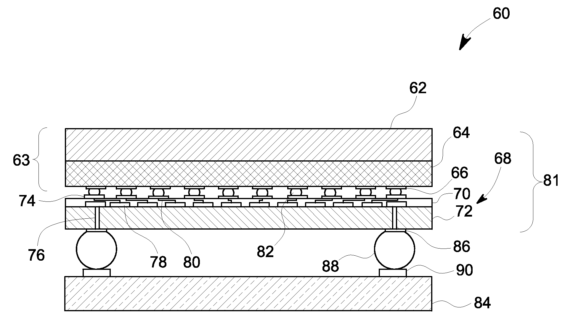
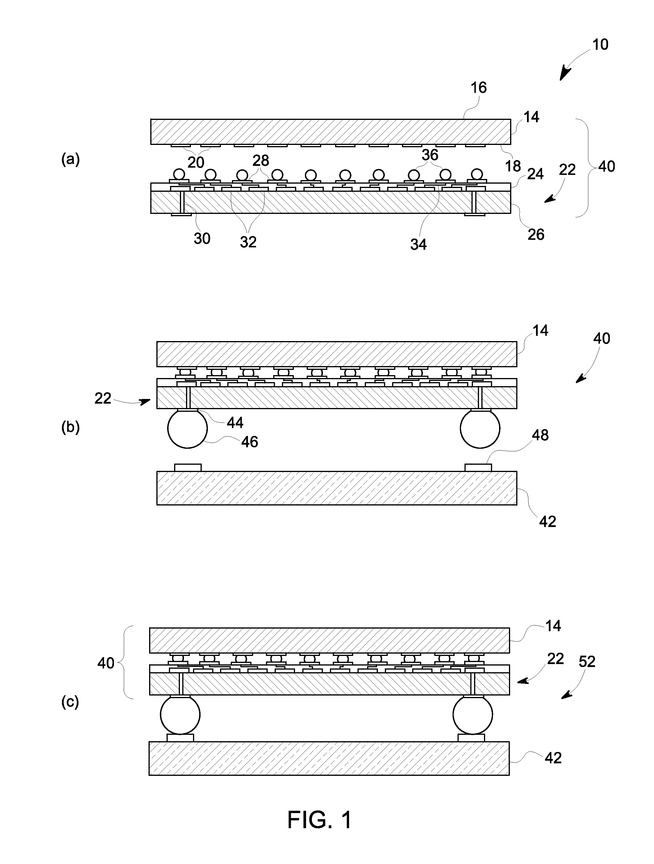
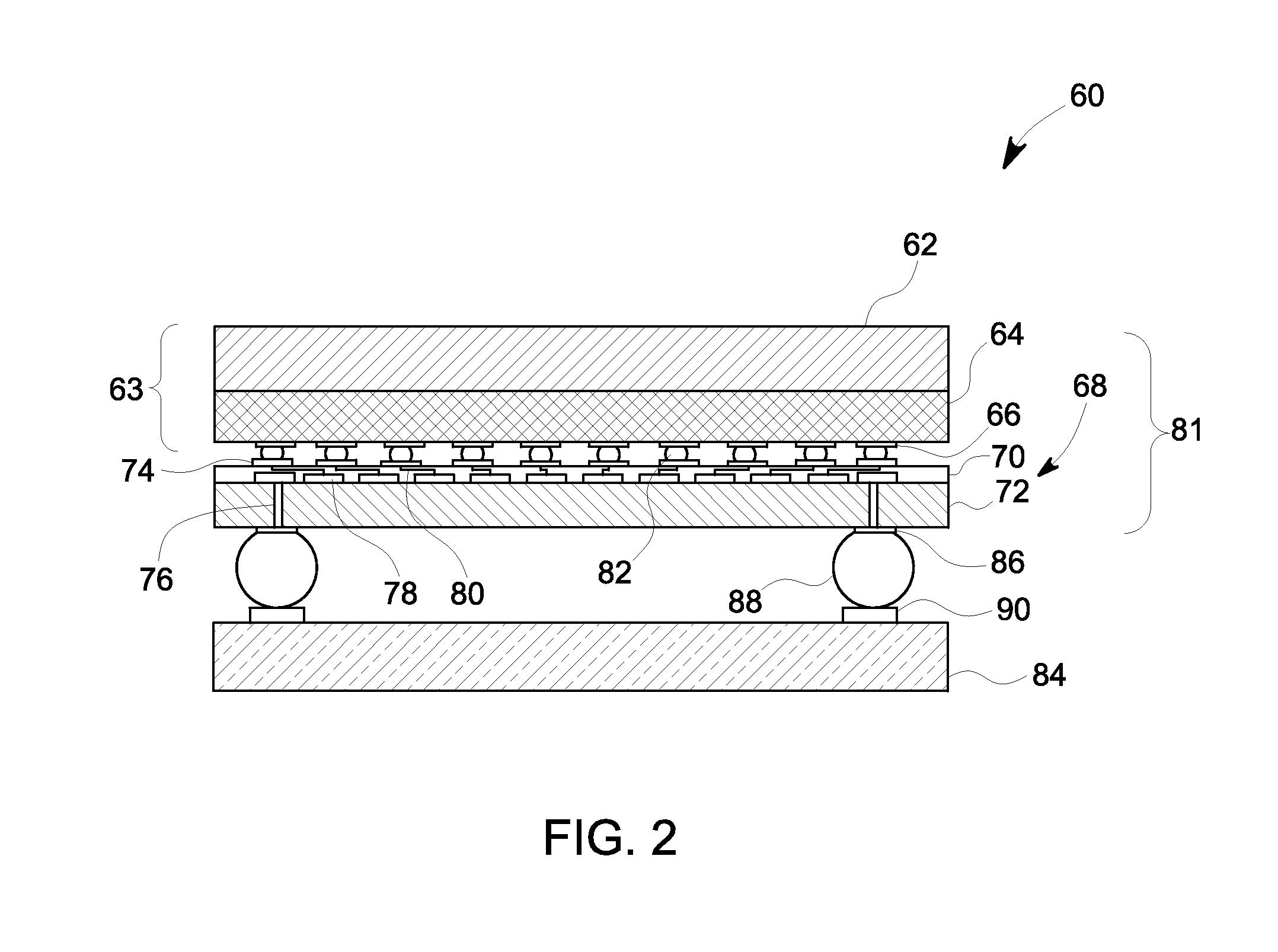
[0059]FIG. 12 is a diagrammatic illustration of another embodiment 206 of a sensor module. In the embodiment illustrated in FIG. 12, a sensor array 207 is indirectly coupled to an integrated circuit 214 via an interposer 208. Accordingly, the sensor array 207 is operationally coupled to the interposer 208. As previously noted, the interposer 208 is an electrical interface routing between one connection to another. In certain embodiments the interposer 208 may include a rigid interposer, while in certain other embodiments, the interposer 208 may include a flexible interposer. By way of example, the rigid interposer may include a FR4 material, while the flexible interposer may include a polyimide. Additionally, the interposer 208 may include a ceramic material or an organic material.

[0060]In a presently contemplated configuration, a second side of the sensor array 207 is coupled to a first side of the interposer 208 to form a sensor array interposer stack. To facilitate this coupling,...

embodiment 280

[0075]In accordance with further aspects of the present technique, the sensor stack 246 may be operationally coupled to the interconnect layer 272 using copper pillars instead of or in combination with the gold stud bumps 278 of FIG. 15. FIG. 16 depicts another embodiment 280 of a sensor module, such as the sensor module 60 of FIG. 2. Particularly, in FIG. 16, the sensor stack 246 (see FIG. 14) is operationally coupled to an interconnect layer, such as the interconnect layer 272 (see FIG. 15) via use of copper pillars 282. Accordingly, copper pillars 282 are disposed on the second set of metal pads 242 to aid in coupling the sensor stack 246 to the interconnect layer 272.

[0076]According to further aspects of the present technique, the various embodiments of the detector modules described hereinabove may be employed in a medical imaging system, such as an ultrasound imaging system. FIG. 17 is a block diagram of an embodiment of an ultrasound imaging system 290. Furthermore, the ultra...


PUM


Abstract

A method for forming a tileable detector array is presented. The method includes forming a detector module, where forming the detector module includes providing a sensor array having a first side and a second side, where the sensor array includes a first plurality of contact pads disposed on the second side of the sensor array, disposing the sensor array on an interconnect layer, where the interconnect layer includes a redistribution layer having a first side and a second side, where the redistribution layer includes a second plurality of contact pads disposed on the first side, an integrated circuit having a plurality of through vias disposed therethrough, where a first side of the integrated circuit is operationally coupled to the second side of the redistribution layer, where the sensor array is disposed on the interconnect layer such that the first plurality of contact pads on the second side of the sensor array are aligned with the second plurality of contact pads on the first side of the redistribution layer, operationally coupling the first plurality of contact pads on the second side of the sensor array to the second plurality of contact pads on the redistribution layer to form a sensor stack, coupling the sensor stack to a substrate to form the detector module, and tiling a plurality of detector modules on a second substrate to form the tileable detector array.

Description

BACKGROUND[0001]Embodiments of the present disclosure relate to sensor arrays, and more particularly to construction of modular sensor arrays.[0002]Sensors or transducers are devices that transform input signals of one form into output signals of a different form. Commonly used transducers include light sensors, heat sensors, and acoustic sensors. An example of an acoustic sensor is an ultrasonic transducer. In ultrasound devices, the transducers transform signals of electrical energy into acoustic energy or produce electrical signals from absorbed sound waves.[0003]Various applications, such as biomedical non-invasive diagnostics and non-destructive testing (NDT) of materials entail the use of sensor arrays, where the sensors are often configured in two-dimensions (that is, the X-Y plane). For example, ultrasonic transducer arrays are used in medical imaging, non-destructive evaluation (NDE) and other applications.[0004]Applications such as medical and industrial imaging, non-destr...

Claims


Application Information

Patent Timeline
Patent Type & Authority Applications(United States)
IPC IPC(8): H01L27/00H01L31/18H01L21/60
CPCH01L27/14634H01L27/14658H01L27/20H01L2224/16225H01L2924/01322H01L2924/1461H01L2924/00A61B8/4483H10N39/00
Inventor TKACZYK, JOHN ERICSMITH, LOWELL SCOTTBAUMGARTNER, CHARLES EDWARDWODNICKI, ROBERT GIDEONFISHER, RAYETTE ANNWOYCHIK, CHARLES GERARDLEWANDOWSKI, ROBERT STEPHEN
Owner GENERAL ELECTRIC CO
Why Eureka
Try Eureka