Method and structure for high q varactor

a varactor and high-q technology, applied in the field of integrated circuits, can solve the problems of many limitations, large cost of ic fabrication facilities, and large cost of devices, and achieve the effects of reducing parasitic resistance and capacitance, high quality factor, and convenient us

Active Publication Date: 2012-06-07
SEMICON MFG INT (SHANGHAI) CORP
View PDF2 Cites 6 Cited by
  • Summary
  • Abstract
  • Description
  • Claims
  • Application Information

AI Technical Summary

Benefits of technology

[0015]Embodiments of the present invention provide many benefits over conventional techniques. For example, the present technique provides an easy to use process that relies upon conventional technology. Embodiments of the present invention provide device layout techniques for reduced parasitic resistance and capacitance. A specific embodiment of the invention provides a method and device for a variable capacitor having a high quality factor (Q).
[0016]A specific embodiment of the invention improves capacitance tuning range of a varactor. Some embodiments of the invention provide layout techniques for achieving high pattern density and design flexibility. Additionally, the method provides a process that is compatible with conventional process technology without substantial modifications to conventional equipment and processes. Depending upon the embodiment, one or more of these benefits may be achieved. These and other benefits will be described in more throughout the present specification and more particularly below.

Problems solved by technology

An IC fabrication facility can cost hundreds of millions, or even billions, of dollars.
Making devices smaller is very challenging, as each process used in IC fabrication has a limit.
Although fabless chip companies and foundry services have increased through the years, many limitations still exist.
However, parasitic resistance and capacitance associated with an MOS capacitor can degrade its performance as a variable capacitor.
Therefore, it is difficult to design a finger-type MOS varactor to achieve both high quality factor and low parasitic capacitance.

Method used


Image

  • Method and structure for high q varactor
  • Method and structure for high q varactor
  • Method and structure for high q varactor

Examples


Embodiment Construction

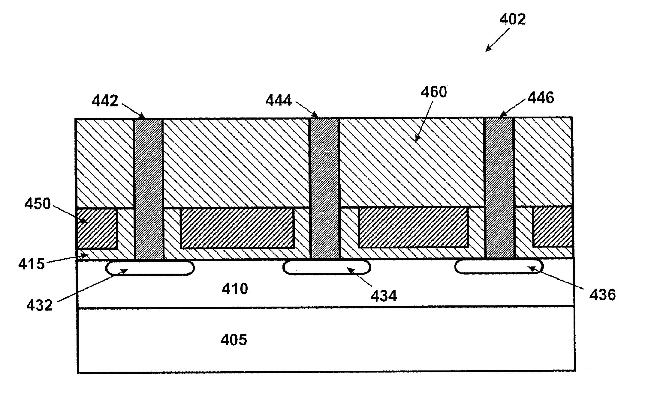
[0025]Embodiments of the present invention provide techniques for fabricating integrated circuit devices. In particular, embodiments of the invention provide a method and device for varactors used in integrated circuits. More particularly, embodiments of the invention provide a method and device for device layout to reduce series resistance and parasitic capacitance. Merely by way of example, the invention has been applied to achieving high quality factor of a variable capacitor for the manufacture of integrated circuits. But it would be recognized that the invention has a much broader range of applicability. For example, the invention can be applied to integrated circuit layout of devices sensitive to parasitic resistance and capacitance, such as resistors, inductors, and transistors, etc.

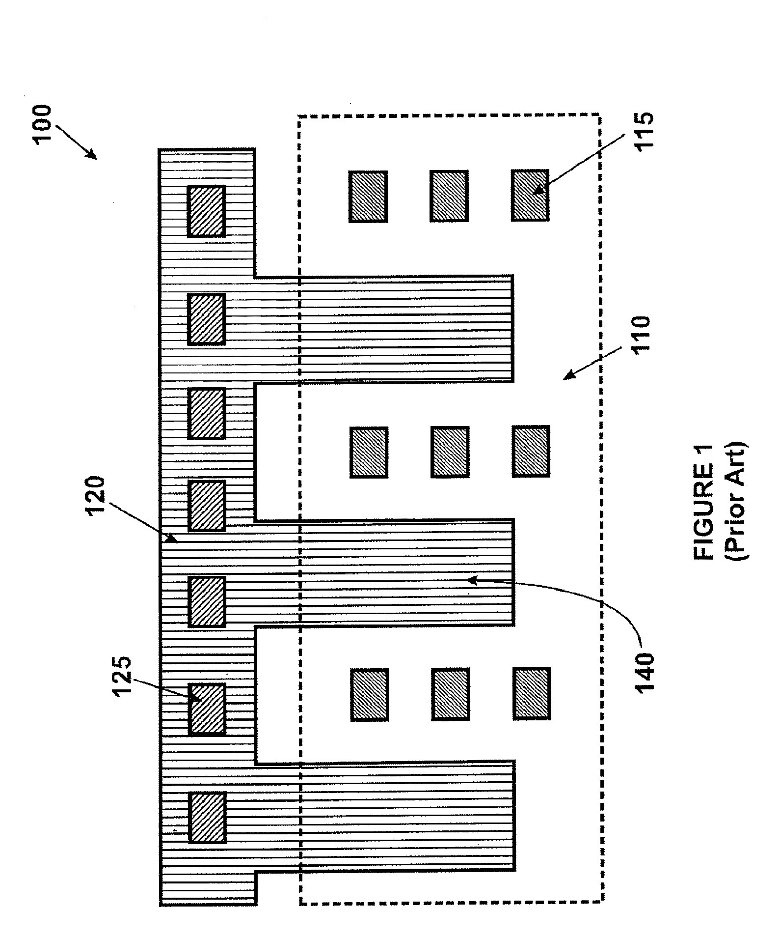
[0026]FIG. 3 is a simplified top-view layout diagram of varactor 300 according to an embodiment of the present invention n. This diagram is merely an example, which should not unduly limit the sco...


PUM


Abstract

A method for forming a variable capacitor includes providing a semiconductor substrate of a first conductivity type and forming an active region of a second conductivity type within the substrate. The method forms a first dielectric layer overlying the active region. The method provides a conductive gate layer over the first dielectric layer and selectively patterns the conductive gate layer to form a plurality of holes in the conductive gate layer. A perimeter of the holes and a spacing between a first and a second holes are selective to provide a high quality factor (Q) of the capacitor. The method implants impurities of the second conductivity type into the active region through the plurality of holes in the conductive layer. The method also includes providing a second dielectric layer and patterning the second dielectric layer to form contacts to the active region and the gate.

Description

CROSS-REFERENCES TO RELATED APPLICATIONS[0001]This application claims priority to Chinese Patent Application No. 201010022580, filed Jan. 8, 2010, which is commonly owned and incorporated by reference herein for all purposes in its entirety.BACKGROUND OF THE INVENTION[0002]Embodiments of the present invention relate to integrated circuits and the processing for the manufacture of semiconductor devices. In particular, embodiments of the invention provide a method and device for varactors used in integrated circuits. More particularly, embodiments of the invention provide a method and device for device layout to reduce series resistance and parasitic capacitance. Merely by way of example, the invention has been applied to achieving high quality factor (Q) of a variable capacitor for the manufacture of integrated circuits. But it would be recognized that the invention has a much broader range of applicability. For example, the invention can be applied to integrated circuit layout of de...

Claims


Application Information

Patent Timeline
Patent Type & Authority Applications(United States)
IPC IPC(8): H01L27/06H01L21/336
CPCH01L29/66181H01L29/94H01L29/93
Inventor CHEN, ZHENLIN, YUNG FENG
Owner SEMICON MFG INT (SHANGHAI) CORP
Why Eureka
Try Eureka