Photoluminescence imaging systems for silicon photovoltaic cell manufacturing

a photoluminescence imaging and photovoltaic cell technology, applied in the field of photoluminescence imaging systems for use, can solve the problem that the existing pl imaging system is not ideally suited to all, and achieve the effect of low image acquisition tim

Inactive Publication Date: 2012-06-07
BT IMAGING PTY LTD
View PDF3 Cites 18 Cited by
  • Summary
  • Abstract
  • Description
  • Claims
  • Application Information

AI Technical Summary

Benefits of technology

[0007]It is an object of the present invention in its preferred form to provide effective photoluminescence imaging systems with low image acquisition times.

Problems solved by technology

However bulk silicon samples (e.g. ingots and bricks) as well as as-cut silicon wafers and PV cell precursors prior to passivation are extremely weak PL emitters because their minority carrier lifetime, on which the PL intensity depends, is limited by surface recombination.
Furthermore even in situations where inspection time is not a critical factor, the applicant has found that different types of silicon samples, e.g. as-cut wafers, surface textured wafers and finished PV cells, each have peculiarities such that existing PL imaging systems are not ideally suited to all of them.

Method used


Image

  • Photoluminescence imaging systems for silicon photovoltaic cell manufacturing
  • Photoluminescence imaging systems for silicon photovoltaic cell manufacturing
  • Photoluminescence imaging systems for silicon photovoltaic cell manufacturing

Examples


Embodiment Construction

[0025]Preferred embodiments of the invention will now be described, by way of example only, with reference to the accompanying drawings.

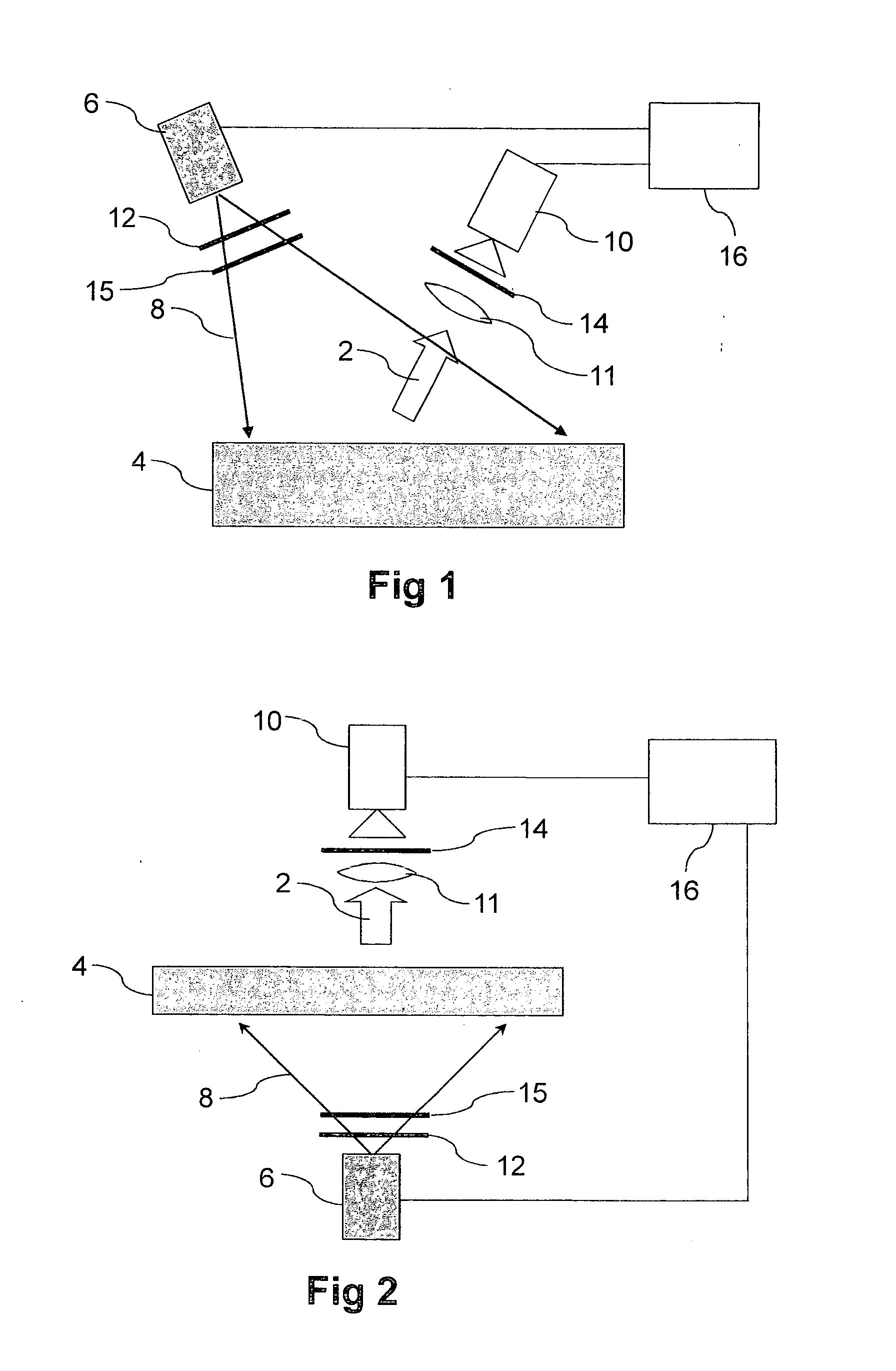
[0026]With its known ability to measure several material parameters of interest to wafer and PV cell manufacturers, photoluminescence (PL) imaging has many existing and potential applications in the PV cell manufacturing industry. PL imaging is already used in stand-alone test and measurement tools, e.g. to investigate poorly performing cells or as a random check of incoming wafer quality, and we believe there are realistic prospects for developing in-line PL imaging systems with a variety of capabilities including wafer sorting and binning, process control feedback (e.g. to correct a defective processing stage) or feed-forward (e.g. to adjust a processing stage in preparation for a different grade of feedstock), either with direct machine control or via a human operator.

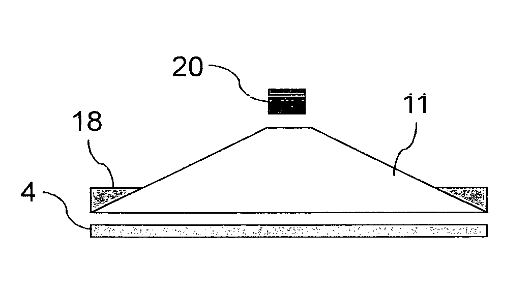
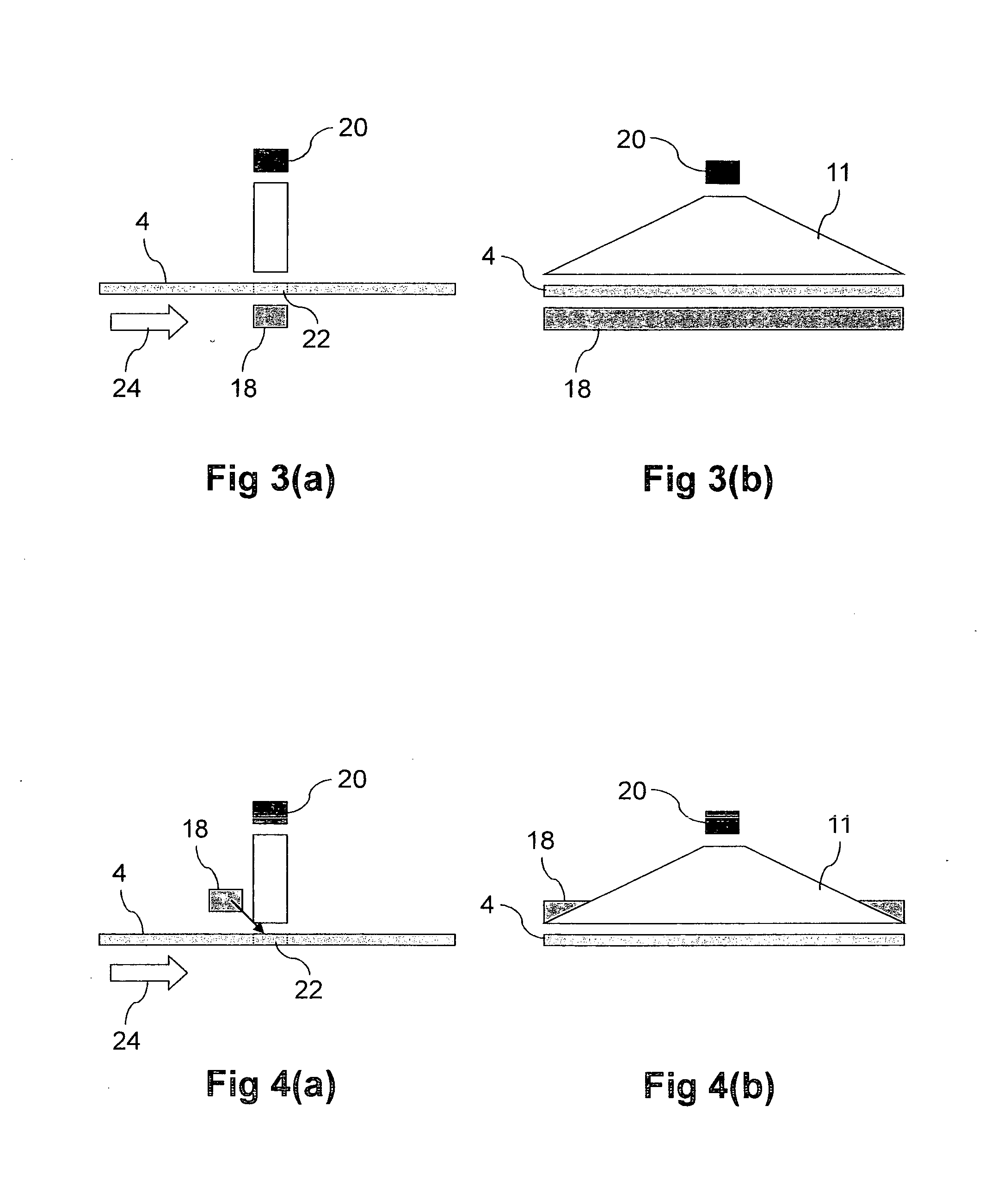
[0027]FIGS. 3(a) and 3(b) show in side view and front view respectively a schem...


PUM

PropertyMeasurementUnit
wavelengthaaaaaaaaaa

Abstract

A method of photoluminence (PL) imaging of a series of silicon wafers, the method including the step of: utilizing incident illumination of a wavelength greater than 808 nm. The present invention further provides a method of analysing silicon semiconductor material utilising various illumination, camera and filter combinations. In some embodiments the PL response is captured by a MOSIR camera. In another embodiment a camera is used to capture the entire PL response and a long pass filter is applied to block a portion of the signal reaching the camera/detector.

Description

FIELD OF THE INVENTION[0001]The present invention relates to photoluminescence imaging systems for use in silicon photovoltaic cell manufacturing.RELATED APPLICATIONS[0002]The present application claims priority from Australian Provisional Patent Application Nos 2009903823, 2009903822 and 2009903813, each filed on 14 Aug. 2009, the contents of which are incorporated herein by reference.BACKGROUND OF THE INVENTION[0003]Any discussion of the prior art throughout this specification should in no way be considered as an admission that such prior art is widely known or forms part of the common general knowledge in the field.[0004]Photoluminescence (PL) imaging, performed for example using apparatus and methods disclosed in PCT Patent Application Publication No WO 2007 / 041758 A1 entitled ‘Method and System for Inspecting Indirect Bandgap Semiconductor Structure’ and incorporated herein by reference, has been shown to be of value for the rapid characterisation of silicon materials and devic...

Claims


Application Information

Patent Timeline
Patent Type & Authority Applications(United States)
IPC IPC(8): G01N21/64H01L21/66
CPCG01N21/6456G01N21/9505G01N21/9501G01N21/6489
Inventor TRUPKE, THORSTENMAXWELL, IAN ANDREWWEBER, JUERGENBARDOS, ROBERT ANDREW
Owner BT IMAGING PTY LTD
Why Eureka
Try Eureka