Pecvd deposition of smooth polysilicon films

a technology of polysilicon and pecvd, which is applied in the direction of chemical vapor deposition coating, liquid surface applicator, coating, etc., can solve the problems of inability to achieve the effect of reducing the thermal budget of the device fabrication process, and affecting the stability of the devi

Inactive Publication Date: 2012-06-07
NOVELLUS SYSTEMS
View PDF8 Cites 45 Cited by
  • Summary
  • Abstract
  • Description
  • Claims
  • Application Information

AI Technical Summary

Benefits of technology

[0010]In some embodiments the smooth silicon films described herein are formed without an anneal. This can be beneficial for the thermal budget of the device fabrication process, and may also be advantageous for structures that have limited stability at higher temperatures. In other embodiments, the films can be annealed after deposition by heating at a temperature of at least about 400° C.

Problems solved by technology

Patterning film stacks for three-dimensional (3D) memory devices can be difficult.
Some conventional atomic layer deposition (ALD), chemical vapor deposition (CVD), high-density plasma chemical vapor deposition (HDP-CVD) and plasma-enhanced chemical vapor deposition (PECVD) processes for depositing film layers may produce unacceptably rough films, cause unacceptable interfacial mixing between film layers, and may have interfacial defects caused by vacuum breaks between successively deposited film layers.
The resulting rough film interfaces and interfacial defects may be magnified by subsequently deposited layers as the film stack is built, so that the top surface of the film stack may be unacceptably rough for downstream patterning processes.
Further, interfacial defects within the film stack may lead to structural and / or electrical defects in the 3D memory device.

Method used


Image

  • Pecvd deposition of smooth polysilicon films
  • Pecvd deposition of smooth polysilicon films
  • Pecvd deposition of smooth polysilicon films

Examples


Embodiment Construction

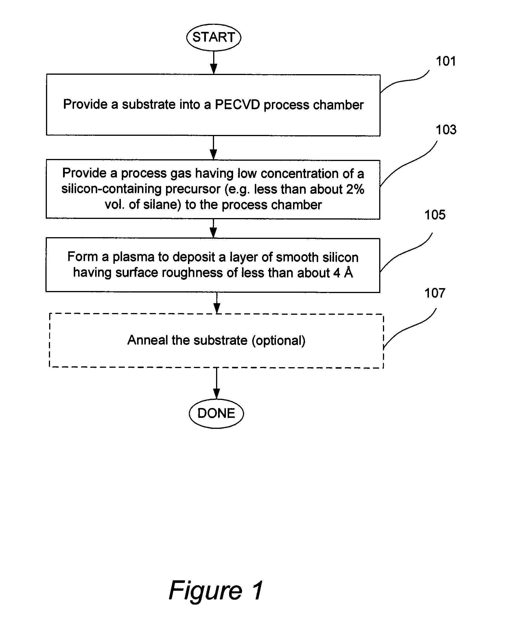
[0026]Reference will now be made in detail to specific embodiments of the invention. Examples of the specific embodiments are illustrated in the accompanying drawings. While the invention will be described in conjunction with these specific embodiments, it will be understood that it is not intended to limit the invention to such specific embodiments. On the contrary, it is intended to cover alternatives, modifications, and equivalents as may be included within the spirit and scope of the invention as defined by the appended claims. In the following description, numerous specific details are set forth in order to provide a thorough understanding of the present invention. The present invention may be practiced without some or all of these specific details. In other instances, well known process operations have not been described in detail in order not to unnecessarily obscure the present invention.

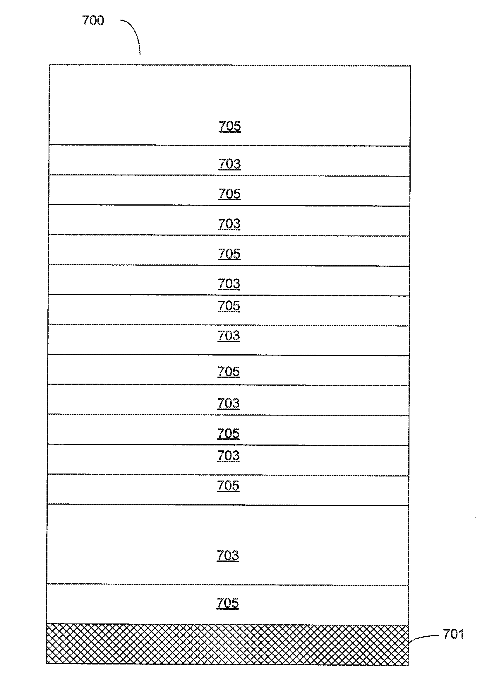
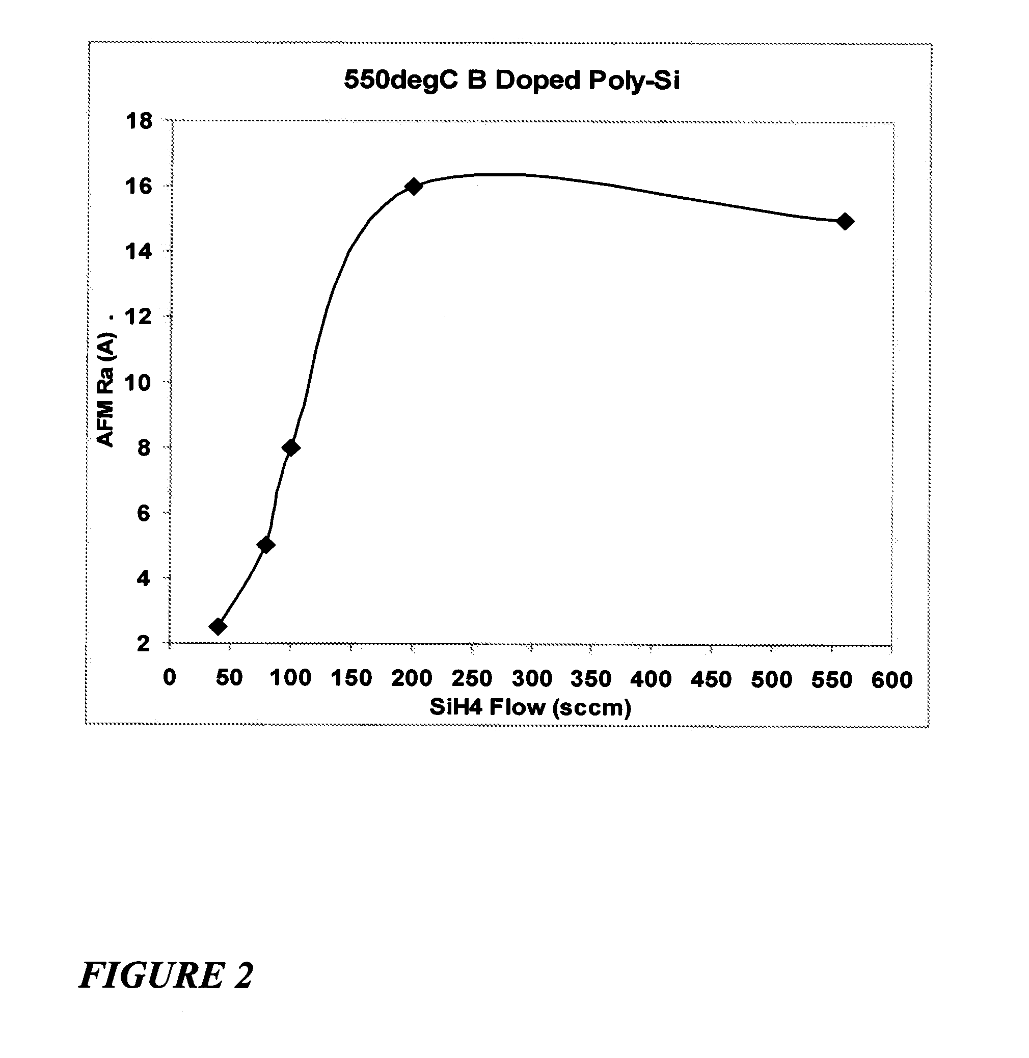
[0027]Smooth silicon and silicon germanium films are provided and methods of forming suc...


PUM

PropertyMeasurementUnit
resistivityaaaaaaaaaa
volume ratioaaaaaaaaaa

Abstract

Smooth silicon and silicon germanium films are deposited by plasma enhanced chemical vapor deposition (PECVD). The films are characterized by roughness (Ra) of less than about 4 Å. In some embodiments, smooth silicon films are undoped and doped polycrystalline silicon films. The dopants can include boron, phosphorus, and arsenic. In some embodiments the smooth polycrystalline silicon films are also highly conductive. For example, boron-doped polycrystalline silicon films having resistivity of less than about 0.015 Ohm cm and Ra of less than about 4 Å can be deposited by PECVD. In some embodiments smooth silicon films are incorporated into stacks of alternating layers of doped and undoped polysilicon, or into stacks of alternating layers of silicon oxide and doped polysilicon employed in memory devices. Smooth films can be deposited using a process gas having a low concentration of silicon-containing precursor and/or a process gas comprising a silicon-containing precursor and H2.

Description

CROSS-REFERENCE TO RELATED APPLICATIONS[0001]This application claims benefit of prior U.S. Provisional Application No. 61 / 420,731 filed Dec. 7, 2010, titled “PECVD DEPOSITION OF SMOOTH POLYSILICON FILMS” naming Fox et al. as inventors, which is herein incorporated by reference in its entirety and for all purposes. This application is also a continuation-in-part of prior U.S. application Ser. No. 12 / 970,853 filed Dec. 16, 2010, titled “SMOOTH SILICON-CONTAINING FILMS” naming Fox et al. as inventors, which claims priority to U.S. Provisional Patent Application Ser. No. 61 / 317,656, titled “IN-SITU PLASMA-ENHANCED CHEMICAL VAPOR DEPOSITION OF FILM STACKS,” and filed on Mar. 25, 2010; U.S. Provisional Patent Application Ser. No. 61 / 382,465, titled “IN-SITU PLASMA-ENHANCED CHEMICAL VAPOR DEPOSITION OF FILM STACKS,” and filed on Sep. 13, 2010; U.S. Provisional Patent Application Ser. No. 61 / 382,468, titled “SMOOTH SILANE-BASED FILMS,” and filed on Sep. 13, 2010; and U.S. Provisional Patent...

Claims


Application Information

Patent Timeline
Patent Type & Authority Applications(United States)
IPC IPC(8): H01L21/20C23C16/52C23C16/50
CPCC23C16/24H01L21/32055C23C16/402C23C16/4401C23C16/45523C23C16/509C23C16/54H01L21/02164H01L21/022H01L21/02274H01L21/0245H01L21/02488H01L21/02507H01L21/02513H01L21/02532H01L21/02587H01L21/0262C23C16/345
Inventor FOX, KEITHSRIRAM, MANDYAMVAN SCHRAVENDIJK, BARTO'LOUGHLIN, JENNIFERWOMACK, JOE
Owner NOVELLUS SYSTEMS
Why Eureka
Try Eureka