Semiconductor device package and method of manufacturing thereof

a technology of semiconductor devices and semiconductor devices, applied in semiconductor devices, semiconductor/solid-state device details, electrical apparatus, etc., can solve the problems of increasing parasitic inductance, limiting operating frequency, and limiting inductance control, so as to minimize parasitic inductance, low parasitic inductance, and high breakdown voltage

Active Publication Date: 2012-06-14
GENERAL ELECTRIC CO
View PDF5 Cites 1 Cited by
  • Summary
  • Abstract
  • Description
  • Claims
  • Application Information

AI Technical Summary

Benefits of technology

[0006]Embodiments of the invention overcome the aforementioned drawbacks by providing a semiconductor device package structure that provides a high breakdown voltage and low parasitic inductance. Multiple passivation layers are formed about a semiconductor device, with the passivation layers having a thickness that provides a desired breakdown voltage for the semiconductor device package and that also provides a minimized parasitic inductance for the semiconductor device package.

Problems solved by technology

However, such dielectric materials often have an increased thickness that may be incompatible with certain POL packaging techniques for the semiconductor diode and, if the thickness is not properly controlled, can lead to increased parasitic inductance.
With respect to providing a low loop inductance between the anode and cathode, challenges arise with controlling the inductance when using conventional packaging technologies.
That is, inherent to conventional packaging technologies are problems associated with the high parasitic inductance of such packages, with this inductance limiting the operating frequency of the semiconductor diode, as it generates losses in the diode during commutation.

Method used


Image

  • Semiconductor device package and method of manufacturing thereof
  • Semiconductor device package and method of manufacturing thereof
  • Semiconductor device package and method of manufacturing thereof

Examples


Embodiment Construction

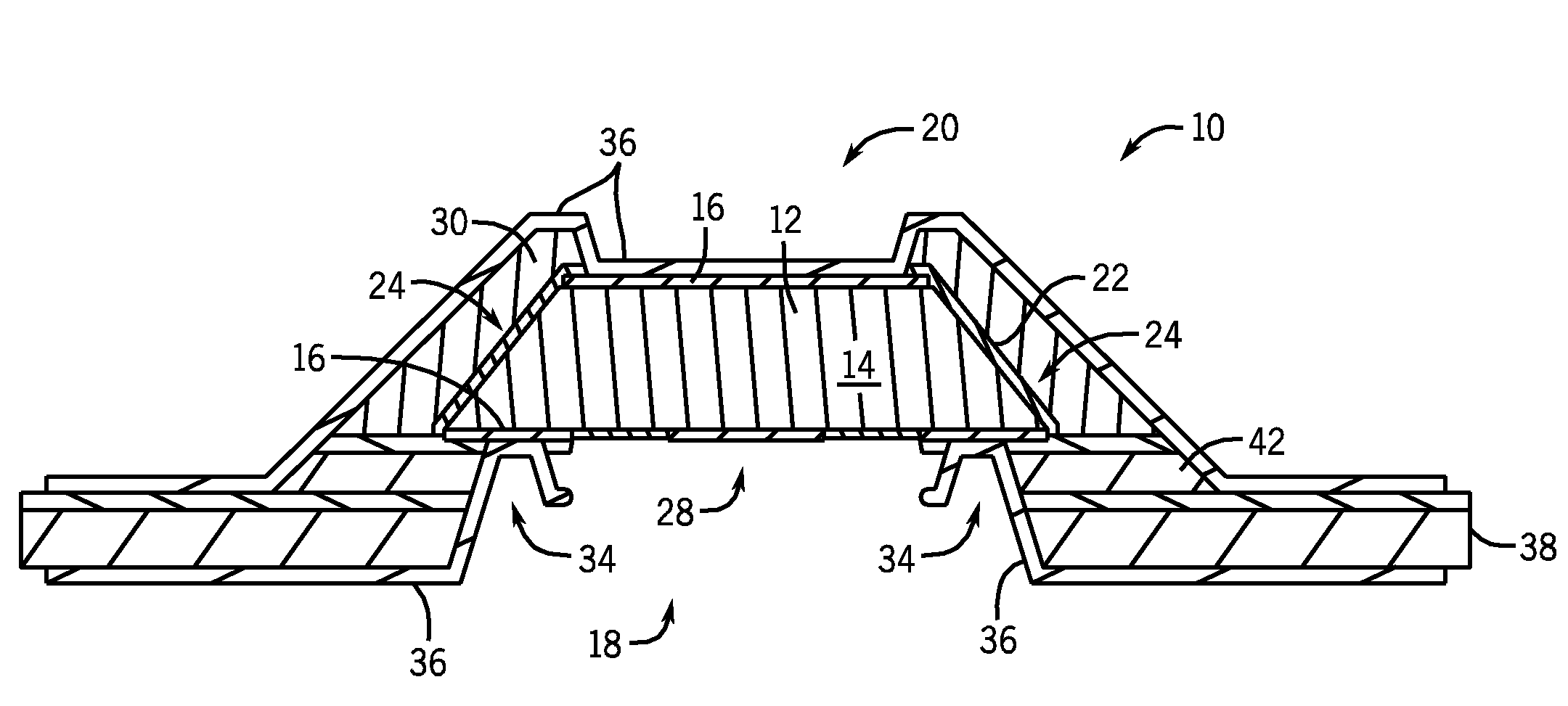
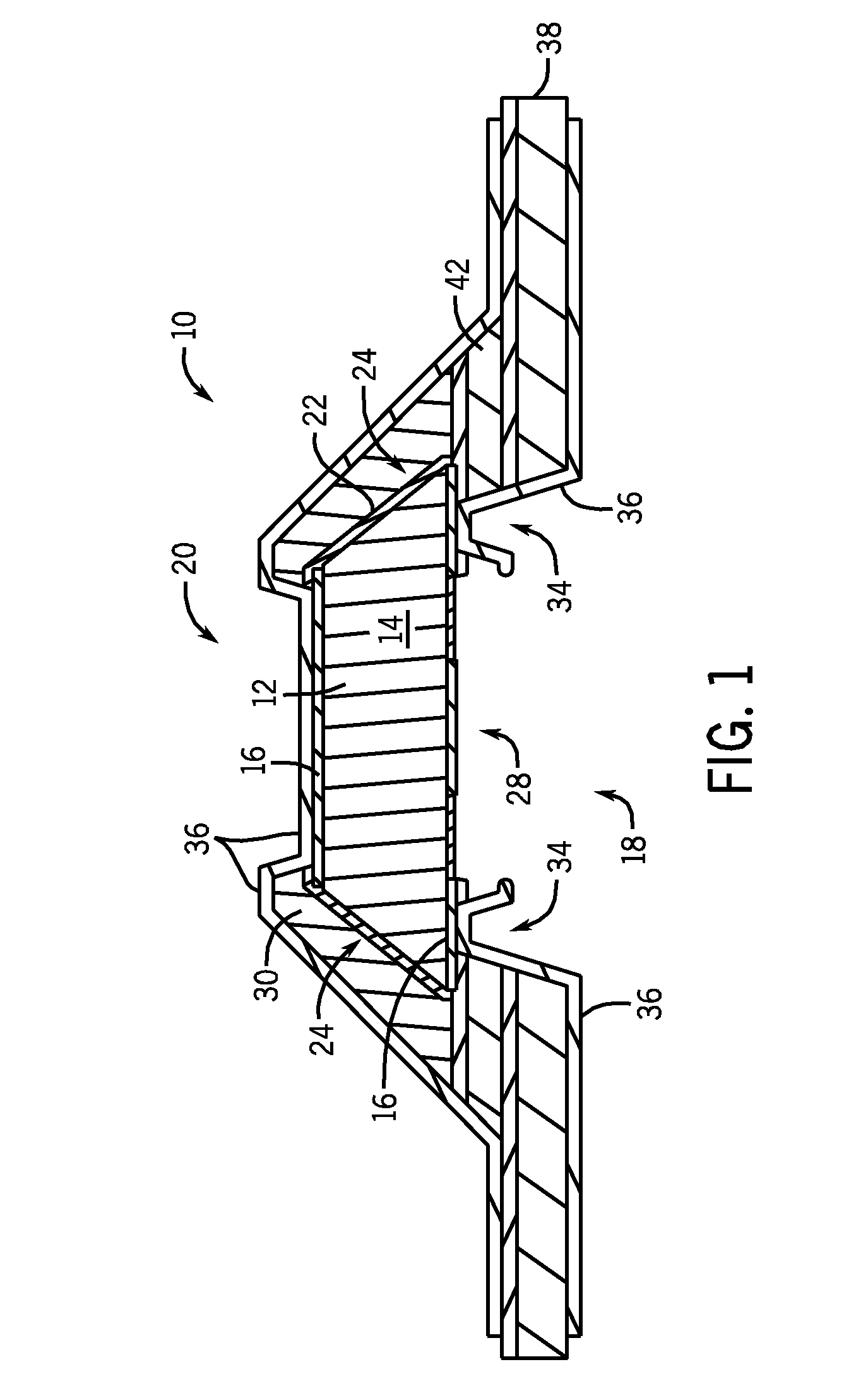
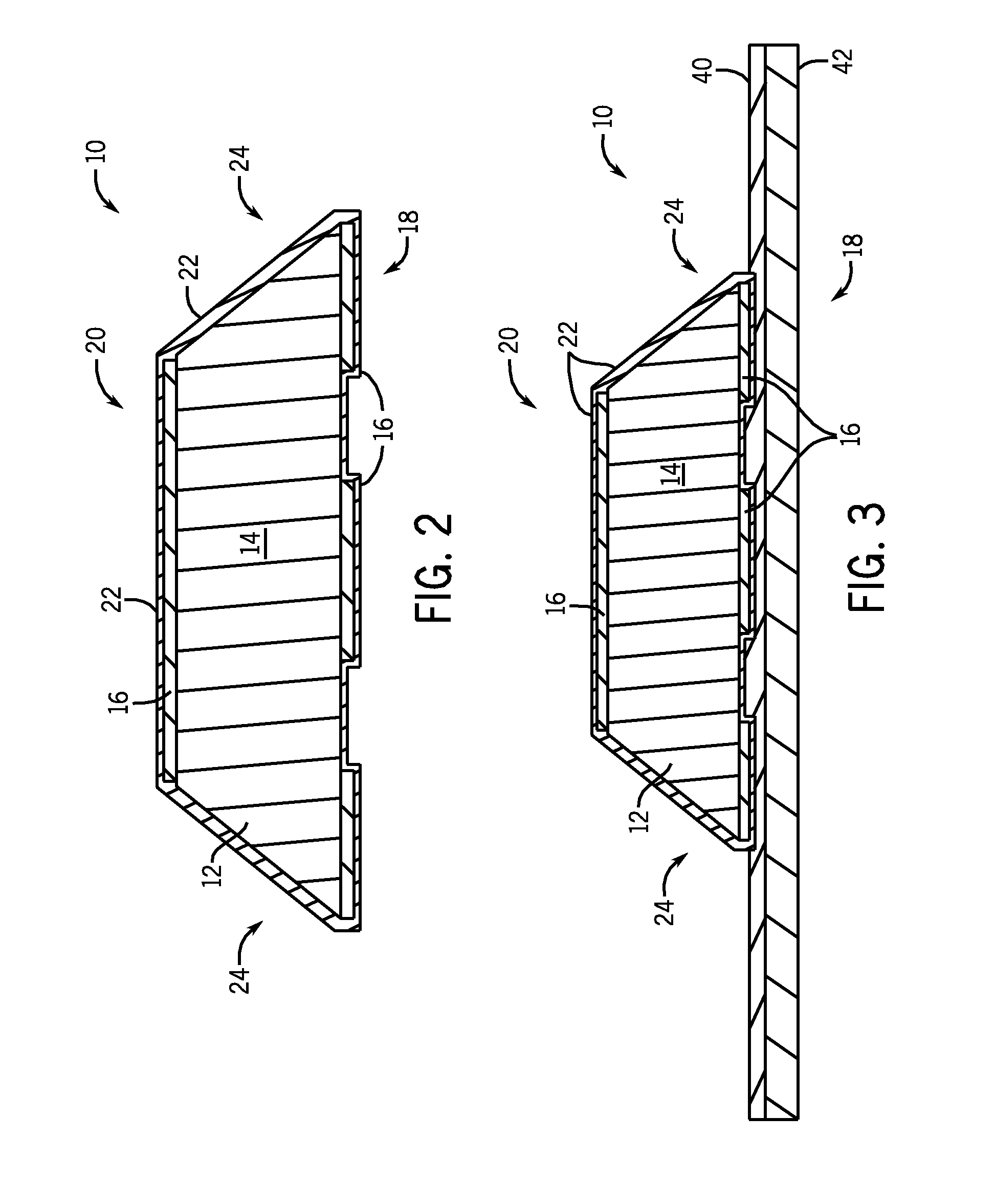
[0017]Embodiments of the present invention provide for a semiconductor device package having a high breakdown voltage and low parasitic inductance, as well as a method of forming such a semiconductor device package. The semiconductor device package is manufactured such that edges of the semiconductor device are passivated using multiple dielectric layers of differing thickness, with an electrical interconnects system being formed to top and bottom surfaces of the semiconductor device.

[0018]Referring to FIG. 1, a semiconductor device package 10 is shown according to an exemplary embodiment of the invention. The semiconductor device package 10 includes a semiconductor device 12 therein that, according to various embodiments, may be in the form of a die, diode, or other electronic device. According to an exemplary embodiment of the invention, semiconductor device 12 is in the form of a high voltage semiconductor diode, such as an optical diode having a back bias in the reverse directio...


PUM


Abstract

A semiconductor device package includes a semiconductor device having connection pads formed thereon, with the connection pads being formed on first and second surfaces of the semiconductor device with edges of the semiconductor device extending therebetween. A first passivation layer is applied on the semiconductor device and a base dielectric laminate is affixed to the first surface of the semiconductor device that has a thickness greater than that of the first passivation layer. A second passivation layer having a thickness greater than that of the first passivation layer is applied over the first passivation layer and the semiconductor device to cover the second surface and the edges of the semiconductor device, and metal interconnects are coupled to the connection pads, with the metal interconnects extending through vias formed through the first and second passivation layers and the base dielectric laminate sheet to form a connection with the connection pads.

Description

BACKGROUND OF THE INVENTION[0001]Embodiments of the invention relate generally to structures and methods for packaging semiconductor devices and, more particularly, to a semiconductor device package structure that provides a high breakdown voltage and low parasitic inductance.[0002]Power semiconductor devices are semiconductor devices used as switches or rectifiers in power electronic circuits, such as switched mode power supplies, for example. Most power semiconductor devices are only used in commutation mode (i.e., they are either on or off), and are therefore optimized for this. One common power semiconductor device is a high voltage power semiconductor diode. A high voltage power semiconductor diode operates on similar principles to its low-power counterpart, but is able to carry a larger amount of current and typically is able to support a larger reverse-bias voltage in the off-state. In use, high voltage power semiconductor diodes are connected to an external circuit by way of...

Claims


Application Information

Patent Timeline
Patent Type & Authority Applications(United States)
IPC IPC(8): H01L23/522H01L21/768
CPCH01L21/56H01L2224/24227H01L23/3171H01L23/3192H01L24/19H01L24/20H01L29/0657H01L2224/24H01L2224/24011H01L2224/2402H01L2224/76155H01L2224/82H01L2224/82105H01L2924/01029H01L2924/01033H01L2924/01082H01L2924/10155H01L2924/01005H01L2924/01006H01L2924/014H01L2224/92144H01L2224/82102H01L23/3164H01L2924/12042H01L2924/12036H01L2924/1204H01L2924/12043H01L2924/00H01L23/48H01L23/28
Inventor BEAUPRE, RICHARD ALFREDMCCONNELEE, PAUL ALANGOWDA, ARUN VIRUPAKSHAGORCZYCA, THOMAS BERT
Owner GENERAL ELECTRIC CO
Why Eureka
Try Eureka