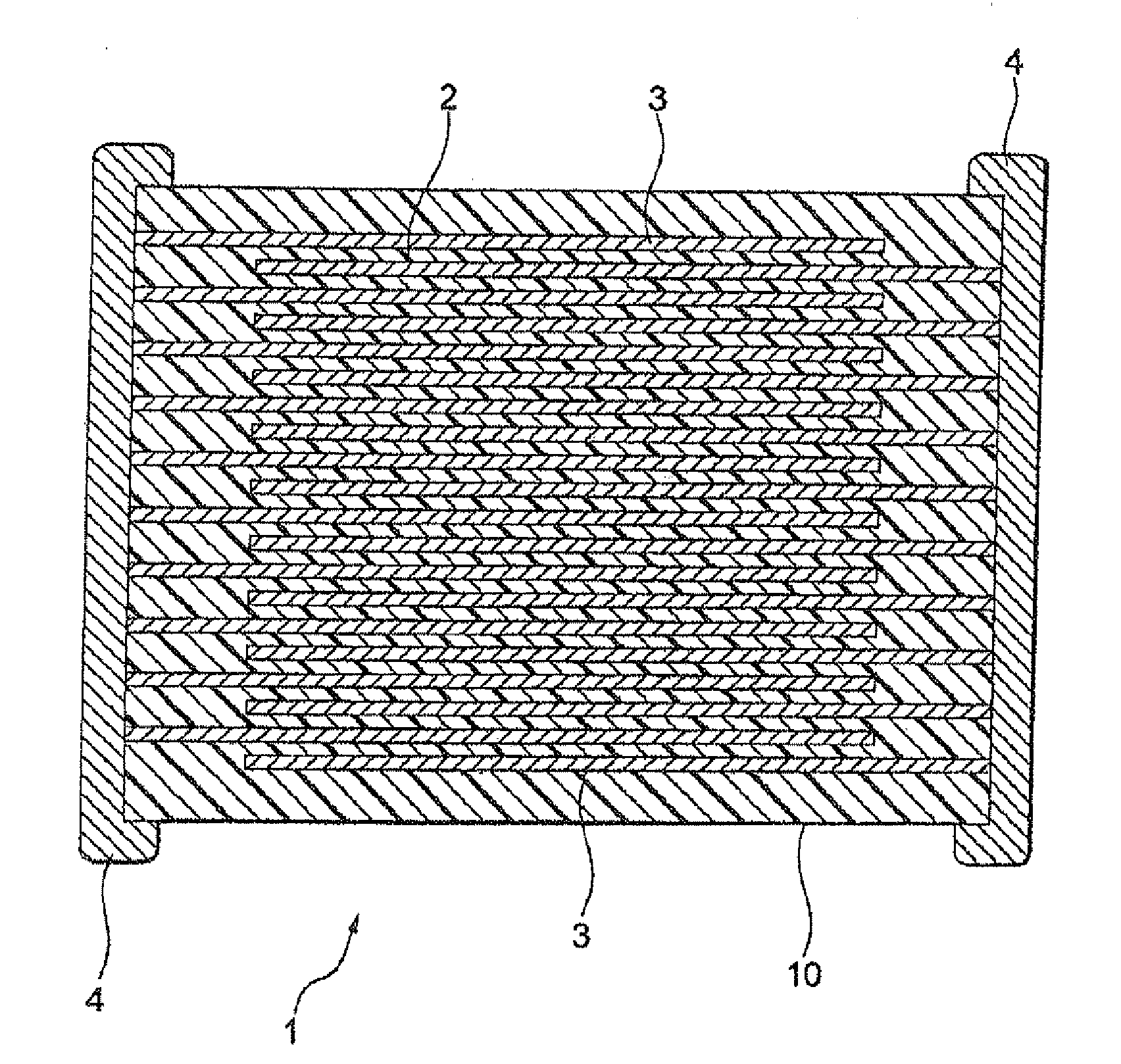

Laminated type ceramic electronic parts

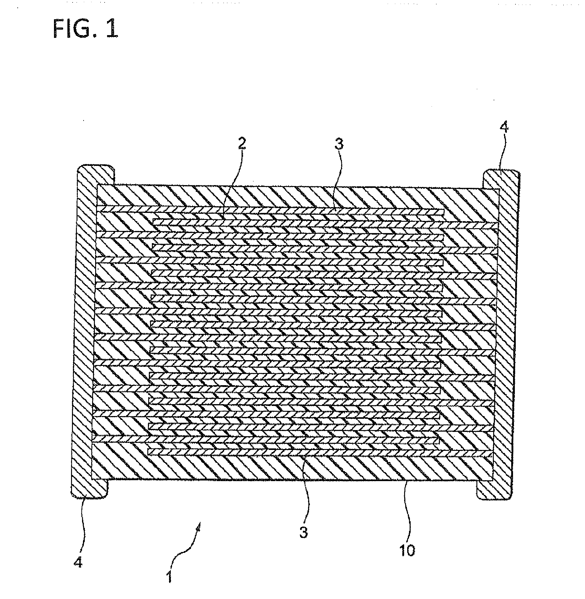
a technology of ceramic electronic parts and laminated ceramics, applied in the direction of fixed capacitors, stacked capacitors, fixed capacitor details, etc., can solve the problems of inability to have a larger capacity and the specific permittivity also declined, so as to achieve the effect of the present invention and further enhance the

Active Publication Date: 2012-06-28
TDK CORPARATION
View PDF1 Cites 48 Cited by
  • Summary
  • Abstract
  • Description
  • Claims
  • Application Information

AI Technical Summary

Benefits of technology

[0017]The present invention was accomplished reflecting such situations, an object is to provide a multilayer ceramic electronic component which can improve dielectric characteristics (particularly, a specific permittivity and a temperature characteristic of a capacitance) regardless of a content of the component included in a dielectric ceramic composition constituting a dielectric layer.
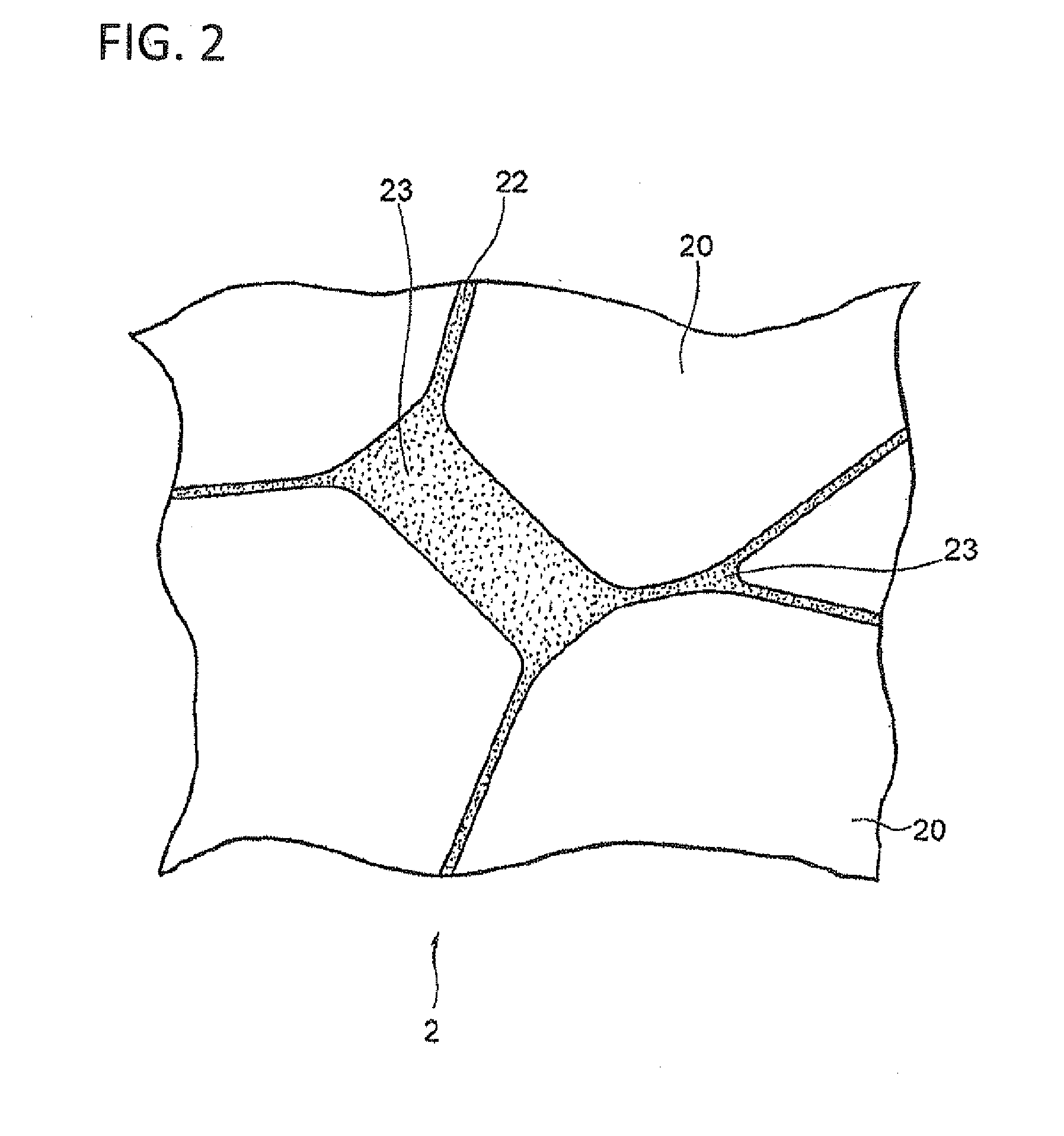
[0021]Thus, in the present invention, contents of the elements which affect the dielectric characteristics when being present in the grain boundary, are controlled to be within above described range. By doing so, a multilayer ceramic electronic component which can improve the dielectric characteristics (the specific permittivity and the temperature characteristic of the capacitance) can be obtained.
[0024]Thus, in the present invention, the content ratio of Ni in the grain boundary is controlled to be within the above range. By doing so, the multilayer ceramic electronic component with improved reliability can be obtained.
[0028]By controlling the content ratios of said elements in the grain boundary as above mentioned, the effect of the present invention can be further enhanced.
[0034]By doing so, the effect of the present invention can be further enhanced.

Problems solved by technology

However, the patent document 1 does not describe the specific content ratio of the above described elements, and the samples of the examples of the patent document 1 had a specific permittivity lower than that of the sample of the comparative example, thus there was problem that it cannot have larger capacity.
However, there was a problem that the specific permittivity also declined when the dielectric layer becomes thinner, as well as the specific permittivity differed depending on the composition of the dielectric ceramic composition.

Method used


Image

  • Laminated type ceramic electronic parts
  • Laminated type ceramic electronic parts
  • Laminated type ceramic electronic parts

Examples


examples

[0127]Hereinafter, the present invention will be explained based on the detailed example; however the present invention is not limited to these examples.

experiment 1

(Experiment 1)

[0128]First, BaTiO3 powder was prepared as the material of ABO3 which is the main component. Also, as the material of the subcomponent, MgCO3 powder as the material of the oxide of Mg, R2O3 powder as the material of the oxide of the R element, (Ba0.6Ca0.4)SiO3 powder (hereinafter referred as BCG) as the material of the oxide including the Si, MnO powder as the material of the oxide of Mn, V2O5 powder as the material of the oxide of V were prepared. Note that, MgCO3 will be included in the dielectric ceramic composition as MgO after firing.

[0129]Next, BaTiO3 powder (average particle diameter:0.3 μm) prepared in the above and the material of the subcomponents were wet pulverized for 15 hours in the ballmill, and dried to obtain the dielectric material. Note that, the added amount of each subcomponent is 2.0 mol of MgO, 1.0 mol of Y2O3, 0.9 mol of BCG, 0.1 mol of MnO, 0.1 mol of V2O5 in terms of each oxides with respect to 100 mol of BaTiO3 as the main component in the di...

experiment 2

(Experiment 2)

[0146]Other than setting the third holding temperature T3 at the third heat treatment to the range in between 650 to 1100° C., the capacitor sample was produced as same as the sample number 4, and the same evaluation as the experiment 1 was carried out, further the high temperature acceleration lifetime (HALT) was evaluated which is shown in the below. The results are shown in Table 2. Note that, in the present example, the same measurement as that of the content ratios of Mg and Si was carried out to the content ratio of Ni in the grain boundary.

(The High Temperature Acceleration Lifetime (HALT))

[0147]The high temperature acceleration lifetime was evaluated by measuring the insulation resistance (IR) over the time while applying the DC voltage under the electric field of 6.3 V / μm at 160° C. In the present example, the time the insulation resistance drops by one order from the start of applying voltage was set as the breakdown time, and mean time to failure was calcula...


PUM

PropertyMeasurementUnit
thicknessaaaaaaaaaa
thicknessaaaaaaaaaa
pressureaaaaaaaaaa

Abstract

A multilayer ceramic electronic component comprising an element body in which a dielectric layer and an internal electrode layer are stacked. The dielectric layer is constituted from a dielectric ceramic composition including; a compound having a perovskite structure expressed by a formula of ABO3 (A is at least one selected from Ba, Ca, and Sr; B is at least one selected from Ti, Zr, and Hf); an oxide of Mg; an oxide of rare earth elements including Sc and Y; and an oxide including Si. The dielectric ceramic composition comprises a plurality of dielectric particles and a grain boundary present in between the dielectric particles. In the grain boundary, when content ratios of Mg and Si are set to D(Mg) and D(Si) respectively, D(Mg) is 0.2 to 1.8 wt % in terms of MgO, and D(Si) is 0.4 to 8.0 wt % in terms of SiO2.

Description

TECHNICAL FIELD[0001]The present invention relate to a multilayer ceramic electronic component, and a multilayer ceramic electronic component which can improve dielectric characteristics (particularly, a specific permittivity and a temperature characteristic of a capacitance) regardless of a content of the component included in a dielectric ceramic composition constituting a dielectric layer.BACKGROUND ART[0002]Recently, as an electronic circuit has become highly densified, there are increasing demands to make an electronic component further compact and to obtain higher performance, and along with that, for example, a multilayer ceramic capacitor has become further compact and has larger capacity, yet further improvement of the characteristics is demanded.[0003]In response to such demands, the improvement of the characteristics is realized by controlling the boundary structure, and by placing different phases other than the main component, in the dielectric ceramic composition const...

Claims


Application Information

Patent Timeline
Patent Type & Authority Applications(United States)
IPC IPC(8): H01G4/12
CPCH01G4/1227H01G4/30H01G4/1281
Inventor TANAKA, HIROBUMIENDO, MAKOTOUEDA, SATOKOUEDA, DAISUKEMUROSAWA, SHOGOYOSHIDA, DAISUKEONO, KENTAOGASAWARA, MINORUKIKUCHI, TATSUYA
Owner TDK CORPARATION
Learn More