Active matrix substrate and display device

a technology of active matrix substrate and display device, which is applied in the direction of semiconductor devices, instruments, electrical apparatus, etc., can solve the problems of display failure, display failure, and inability to inspect the array substrate, so as to achieve sufficient resistance to surge current and narrow picture frame regions

Inactive Publication Date: 2012-07-19
SHARP KK
View PDF1 Cites 1 Cited by
  • Summary
  • Abstract
  • Description
  • Claims
  • Application Information

AI Technical Summary

Benefits of technology

[0039]According to the first and second active matrix substrate of the present invention and the display device of the present invention

Problems solved by technology

Therefore, destruction of a TFT or a defect in the properties of a TFT or the like may be caused by a surge current that results from the build-up and discharge of static electricity or the like in a TFT manufacturing process, a process of rubbing an alignment layer, a process of mounting an external component and the like.
Further, if a voltage that exceeds an allowable withstand voltage by a large margin is applied to the source wiring 102 and/or the gate wiring 103, a surge current may be generated to a

Method used


Image

  • Active matrix substrate and display device
  • Active matrix substrate and display device
  • Active matrix substrate and display device

Examples


embodiment 1

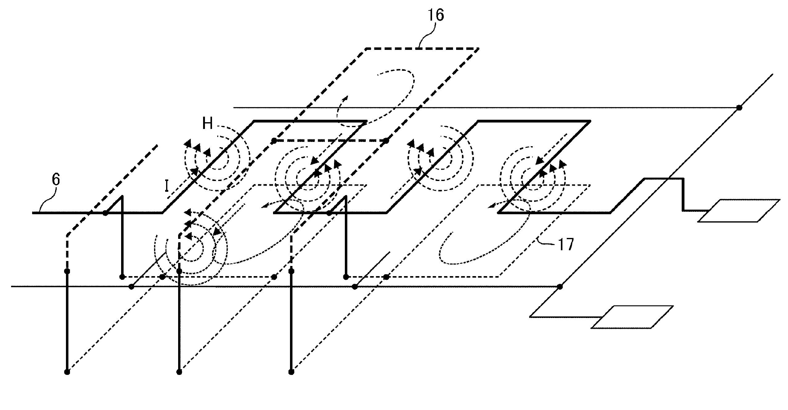
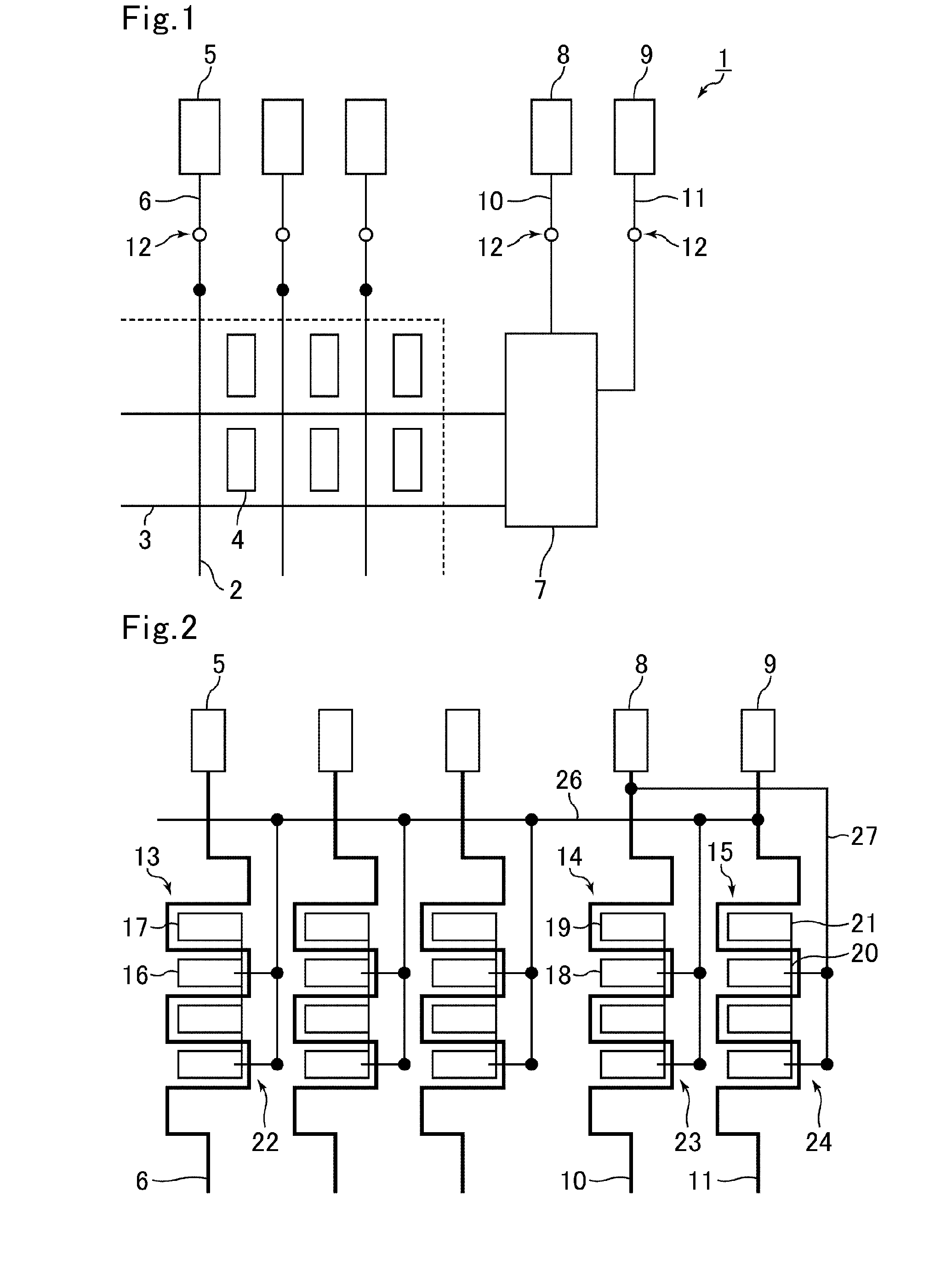
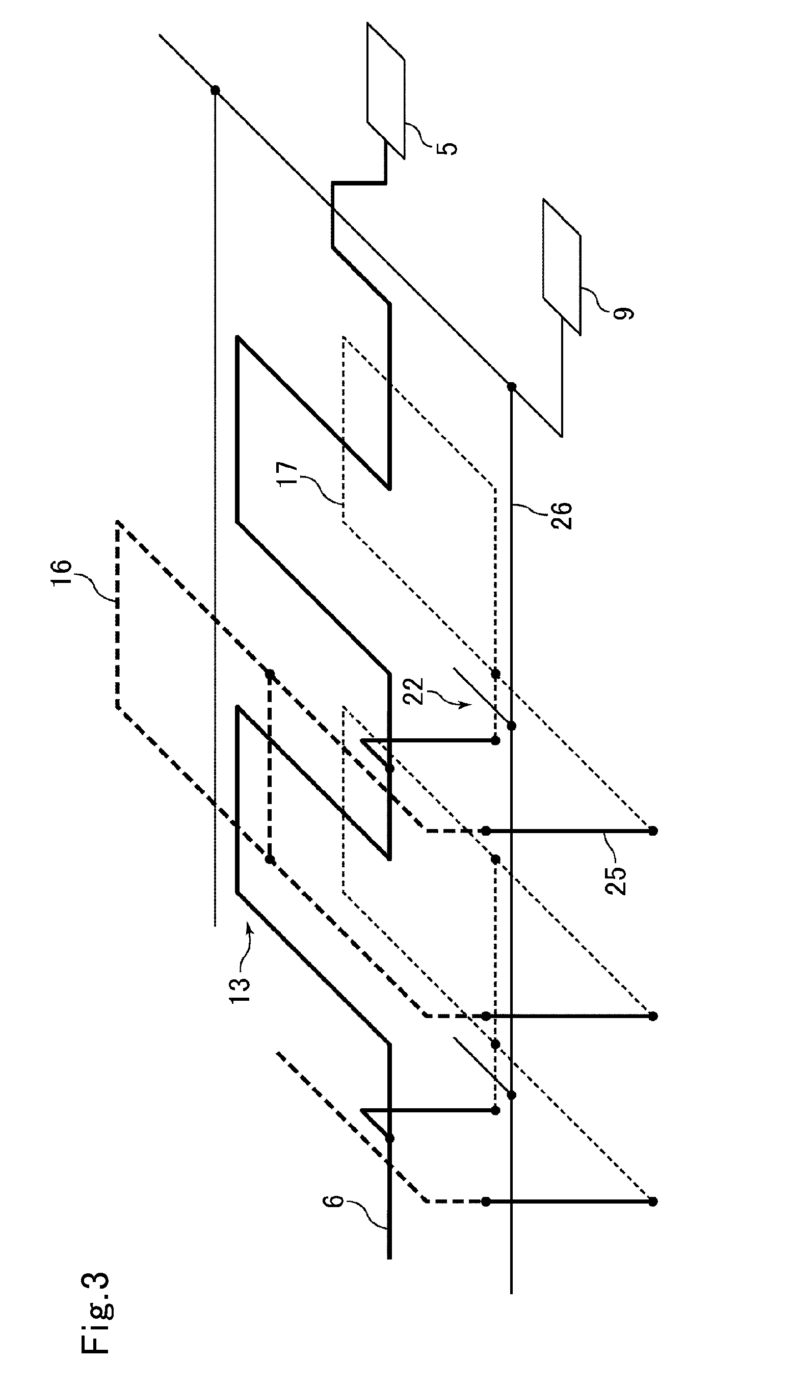
[0054]As shown in FIG. 1, in a display region of an active matrix substrate (array substrate 1) of Embodiment 1, a plurality of source wirings 2 and a plurality of gate wirings 3 are arranged to intersect in a matrix shape through a first interlayer insulation layer. TFTs for pixel switching are arranged at portions at which the source wiring 2 and the gate wiring 3 intersect, and a drain of each TFT is connected to a pixel electrode 4. The pixel electrode 4 faces a common electrode through a liquid crystal layer. The source wiring 2 inputs a signal (image signal) of an image to be displayed on a liquid crystal display panel into a pixel. The gate wiring 3 sequentially inputs scanning signals that control the TFTs from a logic circuit 7 into the TFTs.

[0055]A plurality of input terminals 5 are arranged in a picture-frame region on an extension of the source wiring 2, and the source wirings 2 and the input terminals 5 are connected to each other through lead wires 6 formed in the pict...

embodiment 2

[0076]According to the present embodiment, the only difference with respect to Embodiment 1 is the configuration of the protection circuit, and hence a description of contents that are duplicated in the two embodiments is omitted. Further, in the drawings, members that exert the same functions in the two embodiments are denoted by the same reference symbols.

[0077]As shown in FIG. 8, similarly to Embodiment 1, each lead wire 6 and the power supply lines 10 and 11 have meander-shaped portions 13, 14 and 15, respectively. The lead wires 6 and the power supply lines 10 and 11 are formed by the first conductive film.

[0078]Auxiliary wirings 30, 31 and 32 are formed through the first interlayer insulation layer on the upper layers of the lead wire 6 and power supply lines 10 and 11, respectively. The auxiliary wirings 30 to 32 are formed by the second conductive film. The auxiliary wirings 30 to 32 have meander-shaped portions 33, 34 and 35. The meander-shaped portions 33 to 35 meander in ...


PUM


Abstract

The present invention provides an active matrix substrate and a display device that have sufficient resistance to a surge current without formation of a short ring and that enable narrowing of a picture-frame region. The present invention is an active matrix substrate on which a plurality of pixels are formed in a matrix shape. The active matrix substrate includes, on one principal surface side of the substrate: a terminal; a semiconductor element; wiring that is formed in a picture-frame region of the substrate and that connects the terminal and the semiconductor element; and an annular conductive portion formed through an insulation layer on at least one of an upper layer side and a lower layer side of the wiring. The wiring comprises a meander structure including a meander-shaped portion. A portion of the conductive portion is disposed along the meander-shaped portion.

Description

TECHNICAL FIELD[0001]The present invention relates to an active matrix substrate and a display device. More specifically, the present invention relates to an active matrix substrate that is suitable as an active matrix substrate for which a countermeasure to static electricity that arises during a manufacturing process is required, and to a display device that includes the active matrix substrate.BACKGROUND ART[0002]In conventional active matrix liquid crystal display devices, respectively independent pixels are arranged in a matrix shape in a liquid crystal display panel, and a pixel electrode and a switching element are respectively provided in each of the pixels.[0003]In the above described liquid crystal display devices, a driving voltage is applied to the pixel electrode through the switching element, and liquid crystal is driven by means of a difference in potential between the pixel electrode and a common electrode that is arranged opposite the pixel electrode through the liq...

Claims


Application Information

Patent Timeline
IPC IPC(8): H01L33/08
CPCG02F1/1345G02F2202/22H01L27/0248H01L27/1214H01L33/62H01L33/38H01L2924/0002H01L27/10H01L27/3244H01L2924/00H10K59/12
Inventor TAJIMA, YOSHIMITSU
Owner SHARP KK
Why Eureka
Try Eureka