
Manufacturing method of rigid and flexible composite printed circuit board

a manufacturing method and printed circuit board technology, applied in the manufacture of cables/conductor parts, printed circuits, chemistry apparatuses and processes, etc., can solve the problems of lowering the stability of products, and achieve the effects of improving product quality, product quality and market competiveness, and good conductivity

Inactive Publication Date: 2012-07-26
UNITECH PRINTED CIRCUIT BOARD CORP
View PDF3 Cites 9 Cited by
  • Summary
  • Abstract
  • Description
  • Claims
  • Application Information

AI Technical Summary

Benefits of technology

[0007]Therefore, it is a primary objective of the invention to provide a rigid and flexible composite printed circuit board and a manufacturing method thereof to maintain a good conductivity between the circuit layers of the rigid and soft boards, so as to improve the yield rate, product quality and market competiveness.
[0008]Another objective of the present invention is to provide a way of effectively overcoming the issue of alignment errors for bonding the flexible and rigid substrates.
[0009]A further objective of the present invention is to provide a way of effectively reducing the stacking area of the increased-layer circuit layer and the flexible substrate.
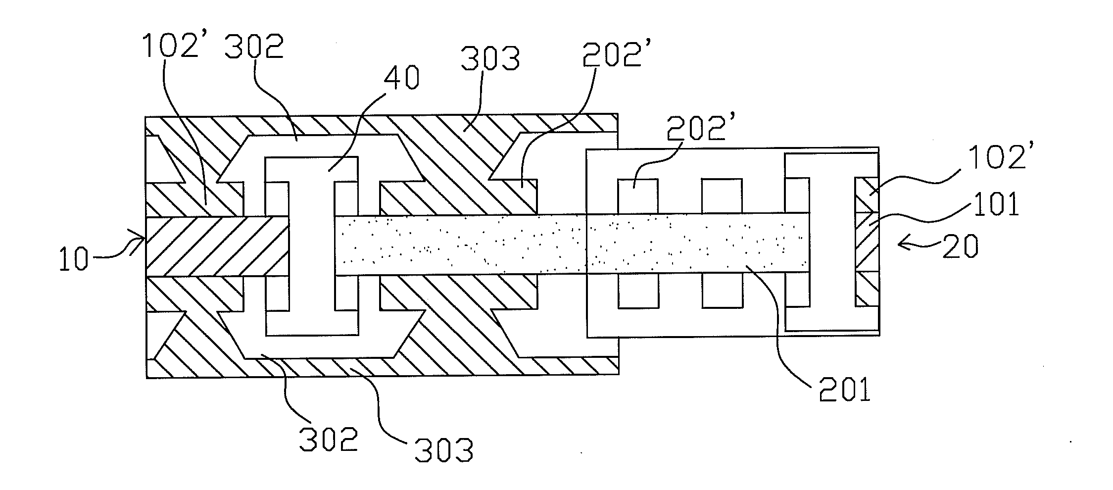
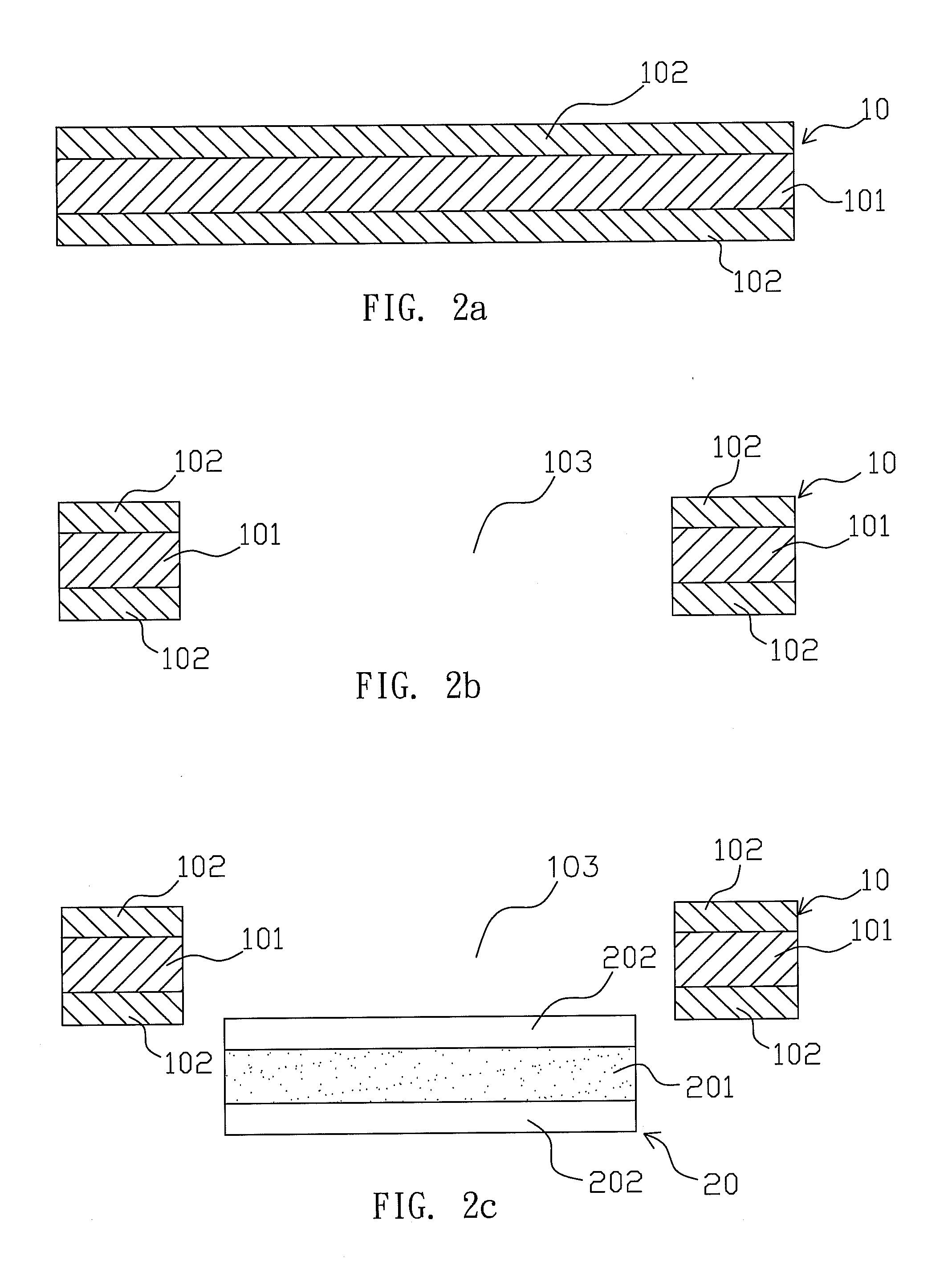
[0010]To achieve the aforementioned objectives, the present invention provides a manufacturing method of rigid and flexible composite printed circuit, and the method comprises the steps of: providing a rigid substrate, wherein the rigid substrate comprises a rigid-board dielectric layer and a rigid-board metal layer, and the rigid-board metal layer is disposed on at least one side of the rigid-board dielectric layer; forming at least one slot on the rigid substrate; installing a flexible substrate in the open slot, and securely bonding the flexible substrate between the flexible substrate and the rigid substrate, wherein the flexible substrate comprises a flexible-board dielectric layer and a flexible-board metal layer, and the flexible-board metal layer is disposed on at least one side of the flexible-board dielectric layer, and the flexible substrate and the rigid substrate are securely bonded with each other; and manufacturing electric circuits on the rigid substrate and the flexible substrate to form rigid and soft boards electric circuit layers simultaneously.

Problems solved by technology

As a result, the stability of the product will be lowered, which is a major difficulty of the manufacture.

Method used


Image

  • Manufacturing method of rigid and flexible composite printed circuit board
  • Manufacturing method of rigid and flexible composite printed circuit board
  • Manufacturing method of rigid and flexible composite printed circuit board

Examples


Embodiment Construction

[0016]The technical contents and characteristics of the image capturing device and its image processing method in accordance with the present invention will be apparent with the detailed description of a preferred embodiment accompanied with related drawings as follows. For simplicity, same numerals are used in the following preferred embodiment to represent respective same elements.

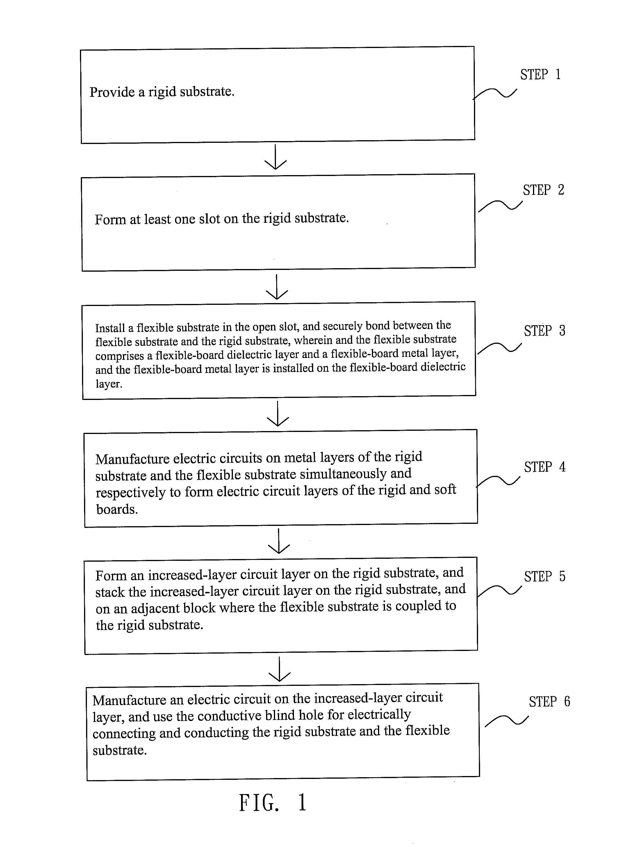
[0017]With reference to FIG. 1 for a flow chart of a manufacturing method of manufacturing method of a rigid and flexible composite printed circuit board in accordance with the present invention, the manufacturing method comprises the following steps:

[0018]Step 1: Provide a rigid substrate.

[0019]Step 2: Form at least one slot on the rigid substrate.

[0020]Step 3: Install a flexible substrate in the open slot, and securely bond between the flexible substrate and the rigid substrate, wherein and the flexible substrate comprises a flexible-board dielectric layer and a flexible-board metal layer, and the flex...


PUM

PropertyMeasurementUnit
Flexibilityaaaaaaaaaa

Abstract

In a manufacturing method of a printed circuit board, a rigid substrate having a rigid-board metal layer is provided, an open slot is formed on the rigid substrate, and a flexible substrate is installed in the open slot, and the flexible substrate and the rigid substrate are securely bonded, and an increased-layer circuit layer is formed after electric circuits are manufactured on the rigid-board and flexible-board metal layers, and stacked on the rigid substrate and on an adjacent block where the flexible substrate is coupled to the rigid substrate, and an electric circuit is manufactured, and the increased-layer circuit layer is provided for electrically connecting and conducting the rigid and flexible substrates to overcome the issue of alignment errors.

Description

BACKGROUND OF THE INVENTION[0001]1. Field of the Invention[0002]The present invention relates to a printed circuit board and a manufacturing method, and more particularly to the rigid and flexible composite printed circuit board and the manufacturing method thereof.[0003]2. Description of Related Art[0004]Speed and density are always factors that drive the promotion and development of high technologies, so that production costs can be reduced, and user requirements can be satisfied. Since electronic products and mobile communication products tend to be developed with a light, thin, short, compact, multifunctional, highly reliable and low-priced design, and these products are developed at a speed of approximately three to five years per generation. With this trend, finding a way of laying the wires on a plane in limited space and extending them to a 3D space is a revolutionary topic for circuit designs of the electronic products.[0005]In addition, a flexible printed circuit board (FP...

Claims


Application Information

Patent Timeline
IPC IPC(8): H05K3/00
CPCH05K3/4652Y10T156/1056H05K2201/09509H05K3/4691
Inventor YEH, MING YILIU, JIA LINWU, CHUNG SHIH
Owner UNITECH PRINTED CIRCUIT BOARD CORP
Learn More