Semiconductor laser device

a semiconductor laser and laser technology, applied in semiconductor lasers, laser details, nanooptics, etc., can solve the problems of insufficient cleavage plane, difficult to realize a semiconductor laser device of a green wavelength range, and inability to make very high light emission layer composition, etc., to achieve the effect of improving design freedom and improving characteristics

Inactive Publication Date: 2012-07-26
ROHM CO LTD
View PDF3 Cites 29 Cited by
  • Summary
  • Abstract
  • Description
  • Claims
  • Application Information

AI Technical Summary

Benefits of technology

[0012]Thus, a second object of the present invention is to provide a semiconductor laser device and a method for manufacturing thereof with which a degree of freedom of selection of laser resonance surfaces can be increased to enable a degree of freedom of design to be increased and a contribution to be made to improvement in characteristics.

Problems solved by technology

However, if the light emitting layer is grown using a group III nitride semiconductor having the m-plane as the major growth surface, the In composition of the light emitting layer cannot be made very high.
It is thus difficult to realize a semiconductor laser device of a green wavelength range (510 nm to 540 nm).
Also, although division guide grooves of a discontinuous pattern are effective for division along a crystal plane of good cleavability, a satisfactory cleavage plane is not necessarily obtained when substrate division is performed along a crystal plane that is not necessarily adequate in cleavability.
A degree of freedom of selection of laser resonance surfaces is thus limited if application of the prior art of United States Patent Application Publication No. 2009 / 0101927 A1 is premised.
Thus, even if a crystal growth surface and a ridge direction of a semiconductor are to be selected in accordance with required specifications, a semiconductor laser device with the required specifications is difficult to realize because the laser resonance surfaces cannot be formed at satisfactory cleavage planes.

Method used


Image

  • Semiconductor laser device
  • Semiconductor laser device
  • Semiconductor laser device

Examples


Embodiment Construction

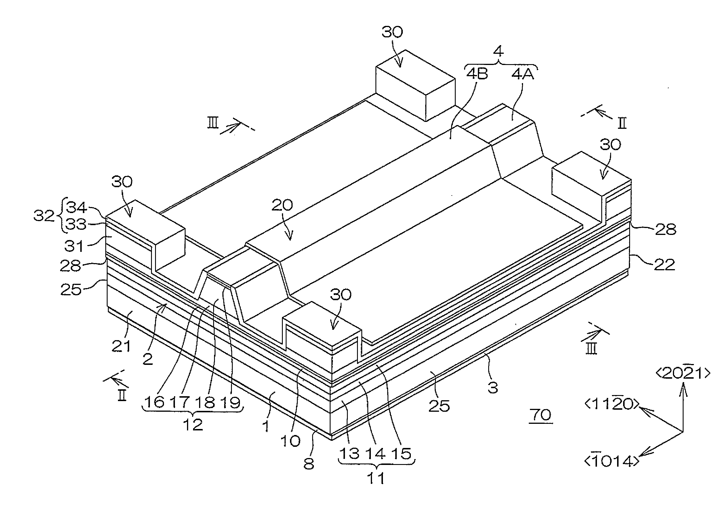
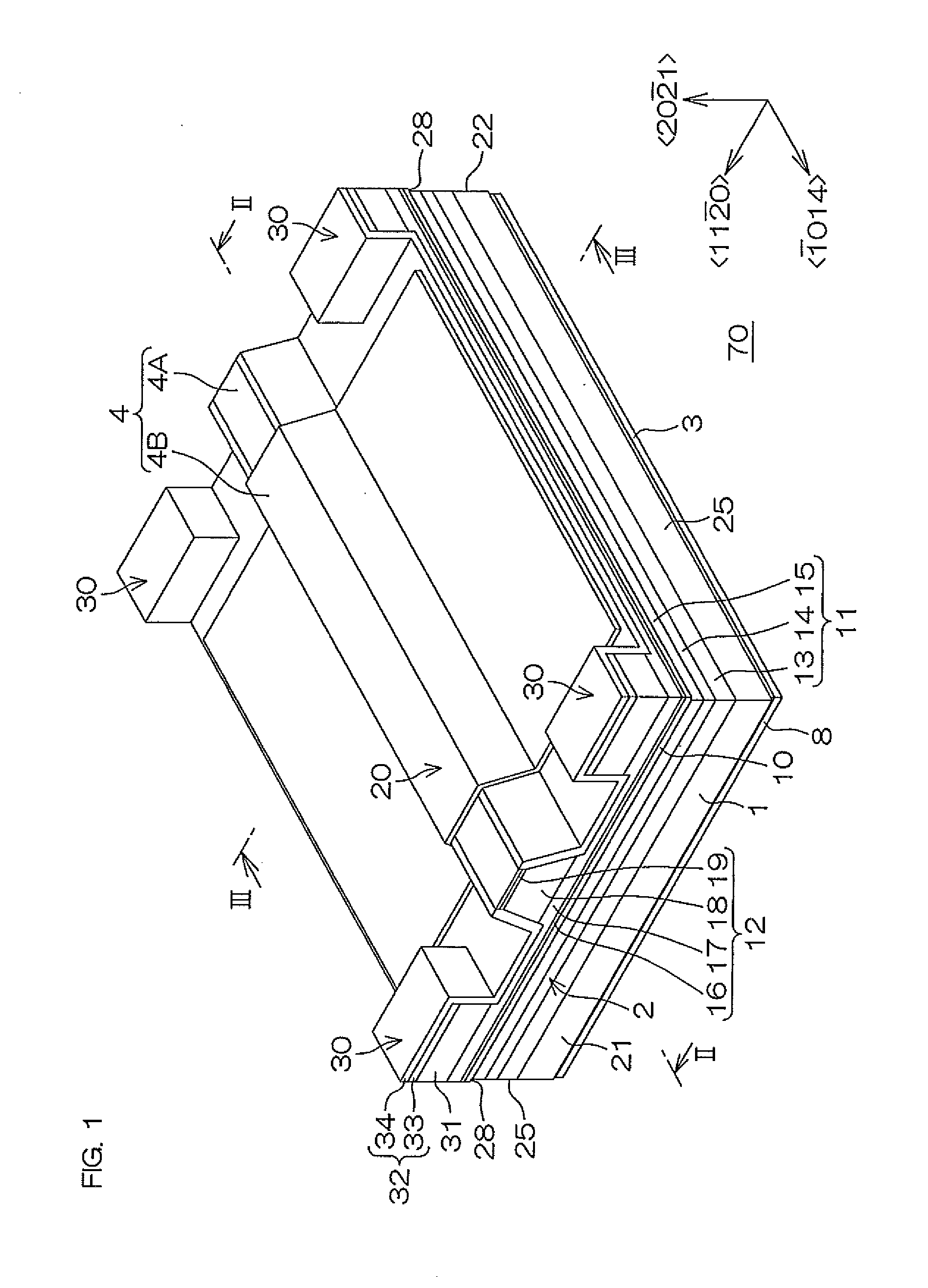
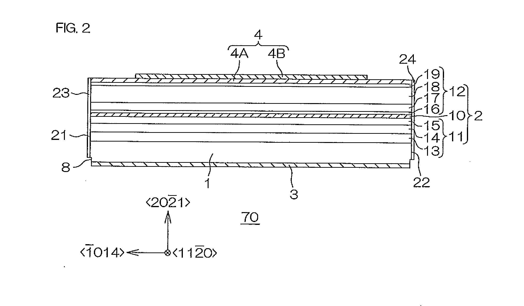
[0035]A preferred embodiment according to a first aspect of the present invention provides a semiconductor laser device including a semiconductor laminate structure made of a group III nitride semiconductor having a semipolar plane as a crystal growth surface. The semiconductor laminate structure includes a light emitting layer that contains In, a p-type guide layer disposed at one side of the light emitting layer, an n-type guide layer disposed at another side of the light emitting layer, a p-type clad layer disposed at an opposite side of the p-type guide layer to the light emitting layer, and an n-type clad layer disposed at an opposite side of the n-type guide layer to the light emitting layer. The semiconductor laminate structure includes a rectilinear waveguide formed parallel to a projection vector of a c-axis onto the crystal growth surface, and a pair of laser resonance surfaces formed of cleavage planes perpendicular to the projection vector.

[0036]According to a most recen...


PUM


Abstract

A semiconductor laser device includes a semiconductor laminate structure that includes a light emitting layer that contains In, a p-type guide layer disposed at one side of the light emitting layer, an n-type guide layer disposed at another side of the light emitting layer; a p-type clad layer disposed at an opposite side of the p-type guide layer to the light emitting layer, and an n-type clad layer disposed at an opposite side of the n-type guide layer to the light emitting layer. The semiconductor laminate structure includes a rectilinear waveguide formed parallel to a projection vector of a c-axis onto the crystal growth surface, and a pair of laser resonance surfaces formed of cleavage planes perpendicular to the projection vector.

Description

BACKGROUND OF THE INVENTION[0001]1. Field of the Invention[0002]The present invention relates to a semiconductor laser device made of a group III nitride semiconductor.[0003]2. Description of Related Art[0004]A group III nitride semiconductor is a group III-V semiconductor in which nitrogen is used as the group V element. Representative examples include aluminum nitride (AlN), gallium nitride (GaN), and indium nitride (InN). The group III nitride semiconductor can generally be expressed as: AlxInyGa1-x-yN (where 0≦X≦1, 0≦Y≦1, and 0≦X+Y≦1).[0005]Laser light sources of short wavelengths, such as blue and green, are coming to be used in such fields as high-density recording onto optical disks as represented by DVDs, image processing, medical equipment, measuring instruments, etc. Such a short-wavelength laser light source is arranged, for example, from a laser diode that uses a GaN semiconductor.[0006]United States Patent Application Publication No. 2009 / 0238227 A1 discloses a semicond...

Claims


Application Information

Patent Timeline
Patent Type & Authority Applications(United States)
IPC IPC(8): H01S5/028H01L21/78
CPCB82Y20/00H01S5/0202H01S5/0287H01S5/2009H01S5/2201H01S2301/176H01S5/3201H01S5/3202H01S5/3211H01S5/34333H01S5/3063H01S5/305H01S5/04254H01S5/320275H01S5/22
Inventor KASHIWAGI, JUNICHIOKAMOTO, KUNIYOSHITANAKA, TAKETOSHIKUBOTA, MASASHI
Owner ROHM CO LTD
Why Eureka
Try Eureka