Organic light emitting diode and manufacturing method thereof

Active Publication Date: 2012-08-02
LG CHEM LTD
8 Cites 341 Cited by

AI-Extracted Technical Summary

Problems solved by technology

NPB, which has currently been used as the hole transporting layer material, has a glass transition temperature of 100° C. or less, and thus it is difficult to apply NPB to an organic light emitting diode requiring a high current.
A LUMO energy level of PEDOT:PSS, which is currently used as a hole trans...

Method used

[0023]In order to enhance the thermal and electrical stability of an organic light emitting diode, hole injection and transporting materials have been developed toward increasing the size of an aryl group of a compound. If a region that the aryl group occupies in a molecule is increased, the overlapping region of the p-orbital is widened, and thus an electrically stable material with minimal change in properties due to the in-and-out of electric charges may be produced. Further, the molecular weight of the molecule itself is increased and thus thermal properties which are endured at high deposition temperature or driving temperature also become excellent.
[0025]In the case of NPB, which is mostly used as a hole transporting material, a paper released by Shumei Liu, et al., (Applied Physics Letters, 97, 083304, 2010) disclosed that another material layer was comprised between NPB as a hole transporting layer and a light emitting layer so as to prevent the deterioration of properties of a diode by light emission of NPB which was in contact with the light emitting layer, and in this case, properties had been improved by 1.6 times in terms of luminance, compared to a diode in which NPB was in direct contact with the light emitting layer. In addition, a paper release by Ming-Te Lin et al., (Solid-State Electronics, 56, 196, 2011) reported that in terms of power efficiency (lm/W), properties had been improved by about 14 times when another material layer was inserted between NPB and the light emitting layer, compared to a diode in which NPB as a hole transporting layer was in direct contact with the light emitting layer.
[0034]The organic material layer comprising the compound having a fluorescent light emitting efficiency equal to or greater than that of NPB is preferably in contact with the light emitting layer. The present invention may provide an organic light emitting diode which suppresses the self-light emission effects of a hole injection material or a hole transporting material to have a high light emitting efficiency and excellent service life by comprising an organic material layer which comprises the compound having the fluorescent light emitting efficiency equal to or greater than that of NPB as a hole injection layer or a hole transporting layer, and comprising the organic material layer which comprises the compound having the fluorescent light emitting efficiency equal to or greater than that of NPB to be in contact with the light emitting layer.
[0079]As shown in FIG. 1, an organic light emitting diode typically consists of a substrate 1, an anode 2, a hole injection layer 5, a hole transportin...

Benefits of technology

[0010]According to exemplary embodiments of the present invention, it is possible to provide an organic light emitting diode having high light emitting efficiency and excellent service life by suppressing self-light emitting e...

Abstract

The present invention relates to a heat emitting body comprising a transparent board, a bus bar, a power supply connected to the bus bar, a heat emitting pattern line provided on the transparent board and electrically connected to the bus bar, and a non-heat emitting pattern line provided on the transparent board and not electrically connected to the bus bar, and a method for manufacturing the same.

Application Domain

Organic chemistryElectroluminescent light sources +4

Technology Topic

PhysicsOLED +4

Image

  • Organic light emitting diode and manufacturing method thereof
  • Organic light emitting diode and manufacturing method thereof
  • Organic light emitting diode and manufacturing method thereof

Examples

  • Experimental program(45)

Example

EXAMPLE
[0243]The compounds used in Examples 1 to 24 and Comparative Examples 1 to 8 are as follows.
[0244]In order to measure the fluorescent light emission efficiencies of cp2 to cp5 as hole injection materials used in Examples and Comparative Examples, each of cp2 to cp5 was deposited to a thickness of 100 nm on a glass substrate by heating each of the materials in vacuum.
[0245]Light having a wavelength of 350 nm was irradiated on a film on which each of cp2 to cp5 was deposited to a thickness of 100 nm by using a 400 W Xenon lamp as a light source, and a PL spectrum was obtained and shown in FIG. 2. In FIG. 2, it is determined that the intensity of max. PL spectra of specimens on which cp3 to cp5 were deposited was higher than that of max. PL spectrum of specimens on which cp2, which is NPB was deposited.

Example

Example 1
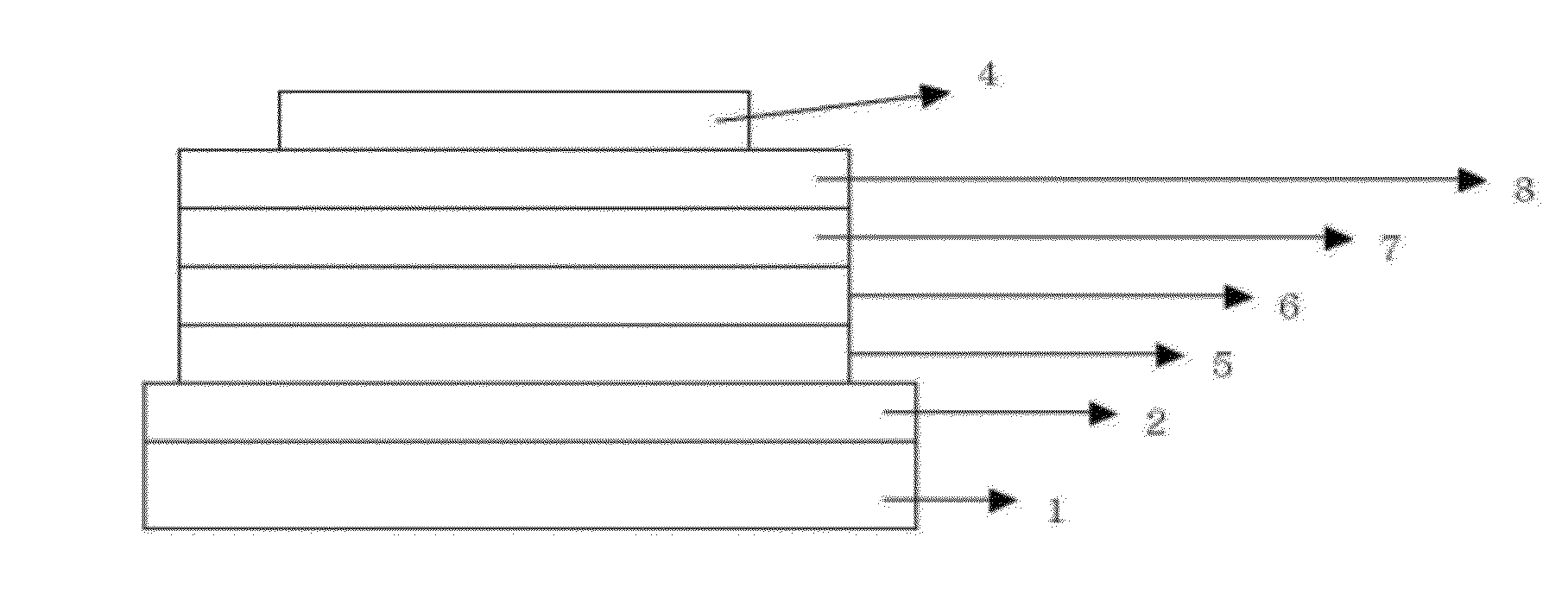
[0246]A transparent electrode (Indium Tin Oxide) was deposited as a hole injection electrode to a thickness of 100 nm on a glass substrate, and was subjected to oxygen plasma at a pressure of 30 mTorr and a power of 80 w for 30 sec. [cp1] was deposited to a thickness of 30 nm thereon by heating the compound [cp1] in vacuum. [cp2] which was NPB as a hole injection layer was deposited to a thickness of 100 nm thereon. [cp7] as a light emitting dopant was doped in an amount of 16% while [cp6] as a light emitting layer was deposited to a thickness of 30 nm thereon. Subsequently, an organic light emitting diode was manufactured by depositing [cp8], which is a part of Formula 1, as an electron transporting and injection layer to a thickness of 20 nm thereon, depositing LiF as an electron injection layer to a thickness of 1 nm thereon, and depositing Al as an electron injection electrode to a thickness of 150 nm thereon.

Example

Example 2
[0247]An organic light emitting diode was manufactured in the same manner as in Example 1, except that [cp3], which is a part of Formula 4, was used instead of [cp2] which was NPB as a hole transporting layer in Example 1.

PUM

PropertyMeasurementUnit
Fraction0.13fraction
Efficiency
Phosphorescence quantum yield

Description & Claims & Application Information

We can also present the details of the Description, Claims and Application information to help users get a comprehensive understanding of the technical details of the patent, such as background art, summary of invention, brief description of drawings, description of embodiments, and other original content. On the other hand, users can also determine the specific scope of protection of the technology through the list of claims; as well as understand the changes in the life cycle of the technology with the presentation of the patent timeline. Login to view more.

Similar technology patents

Pyrene compound and organic light emitting device

InactiveUS20080119671A1high light emit efficiencyhigh durability
Owner:CANON KK

Organic electroluminescent element, displaying apparatus, light emitting method, displaying method and transparent substrate

InactiveUS6903506B2high light emit efficiencylow moisture permeability
Owner:KONICA CORP

Organic EL display device having organic soluble derivative layer

InactiveUS20050153166A1high light emit efficiencyimproved life span
Owner:SAMSUNG DISPLAY CO LTD

Light-emitting material, organic light-emitting device, and compound

ActiveUS20170047522A1high light emit efficiency
Owner:KYULUX INC

Light emitting device

InactiveUS20120236229A1high light emit efficiency
Owner:PANASONIC CORP

Classification and recommendation of technical efficacy words

  • high light emit efficiency

Light emitting apparatus

InactiveUS20070252166A1high light emit efficiencyhigh effect
Owner:DELTA ELECTRONICS INC

Organic Electroluminescence Element Material, Organic Electroluminescence Element, Display Device and Lighting Apparatus

ActiveUS20090302745A1high light emit efficiencylong light emission life
Owner:MERCK PATENT GMBH

Display device

InactiveUS20090115952A1high light emit efficiencylarge aperture area
Owner:SHARP KK

Alternating current light emitting device

ActiveUS20090160370A1high light emit efficiencyimprove flicker
Owner:EPISTAR CORP

Organic electroluminescent element, displaying apparatus, light emitting method, displaying method and transparent substrate

InactiveUS6903506B2high light emit efficiencylow moisture permeability
Owner:KONICA CORP
Why Eureka
Try Eureka