Semiconductor device and method for manufacturing the same

Active Publication Date: 2012-08-02
SEMICON ENERGY LAB CO LTD
View PDF6 Cites 14 Cited by
  • Summary
  • Abstract
  • Description
  • Claims
  • Application Information

AI Technical Summary

Benefits of technology

[0022]According to one embodiment of the disclosed invention, the number of photolithography steps used for manufacturing

Problems solved by technology

When the step of etching the oxide semiconductor layer is skipped, the oxid

Method used


Image

  • Semiconductor device and method for manufacturing the same
  • Semiconductor device and method for manufacturing the same
  • Semiconductor device and method for manufacturing the same

Examples


example

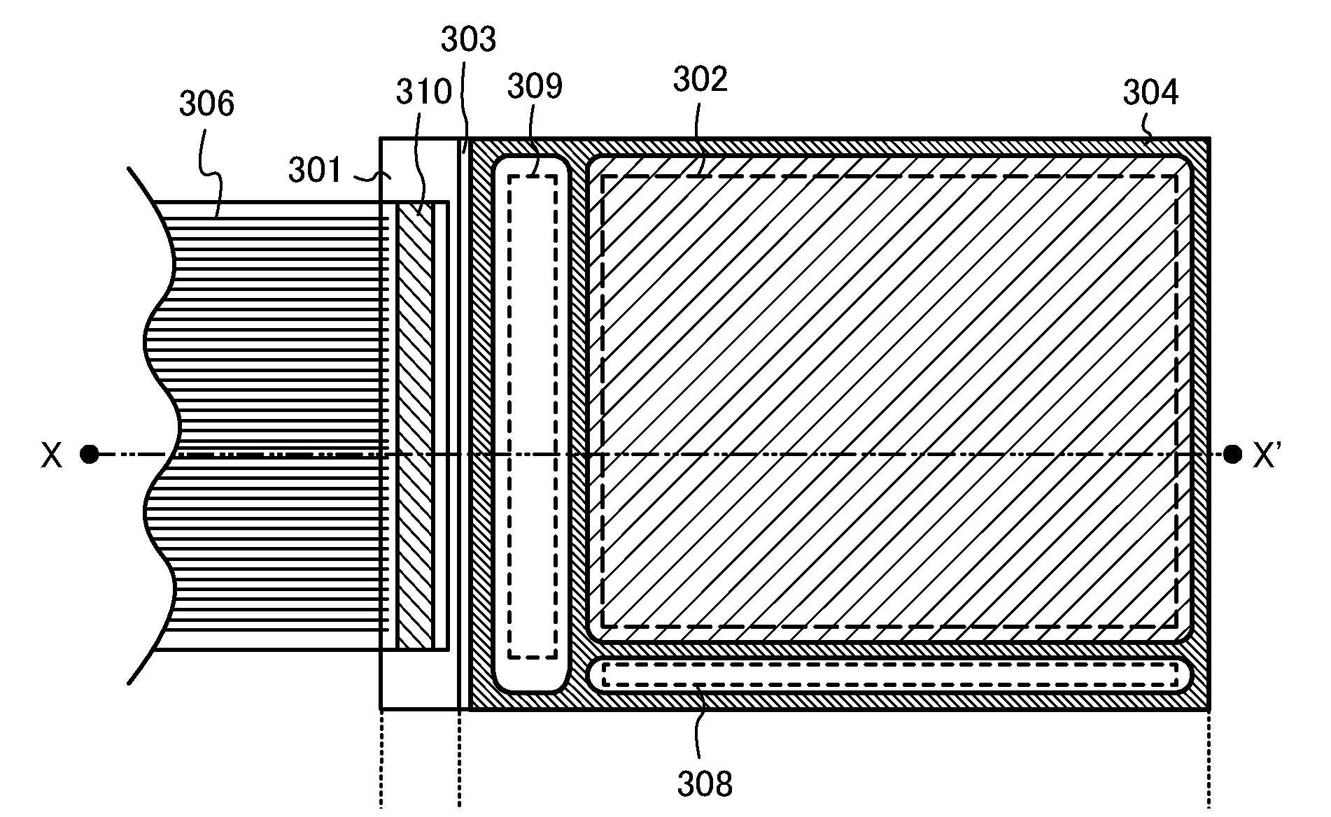
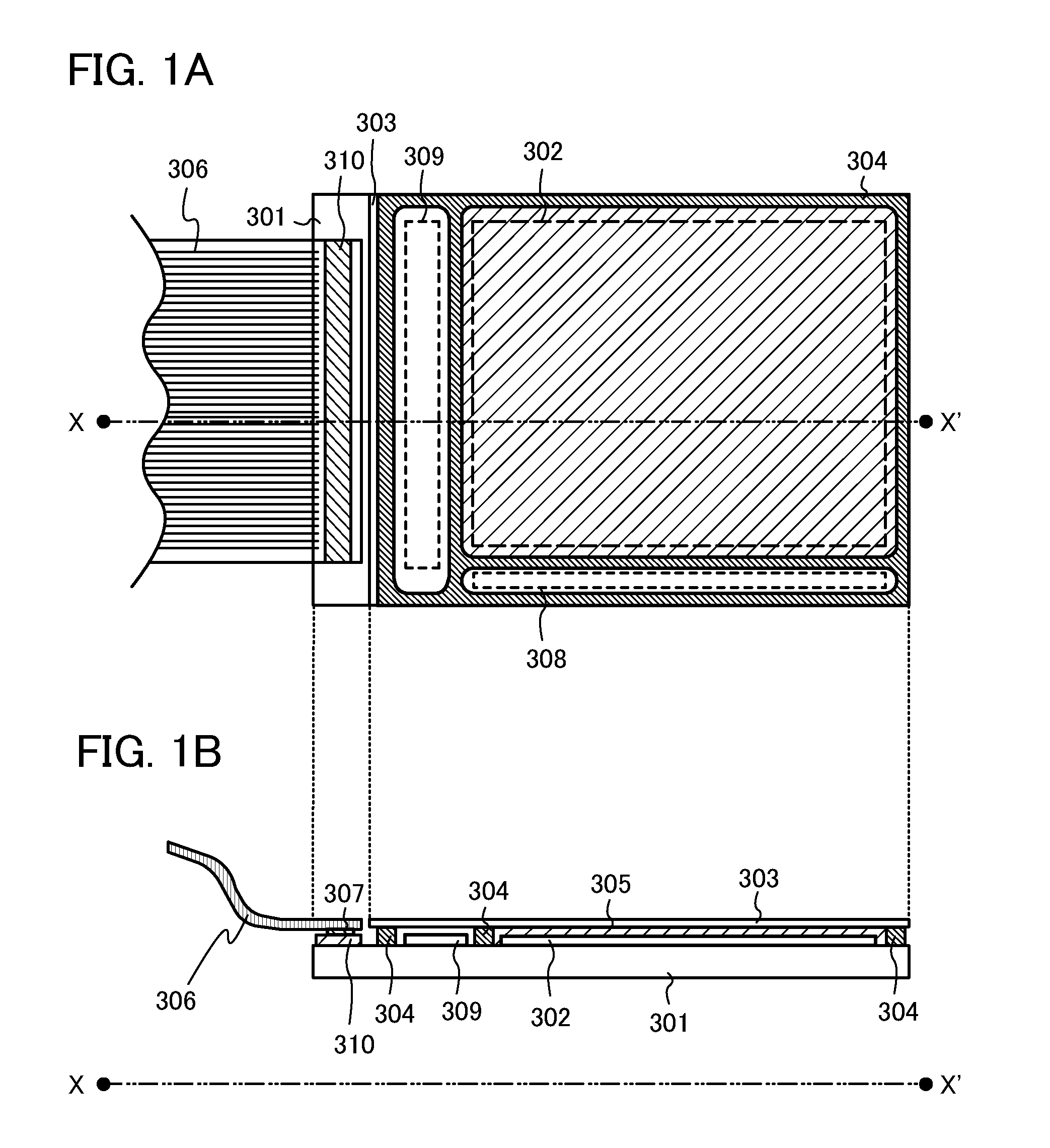
[0147]In FIGS. 8A and 8B and FIGS. 9A and 9B, characteristics of a transistor as a comparative example and an oxide semiconductor transistor manufactured according to the description of the embodiment are shown.

[0148]In this example, a gate-bias stress test was performed on the transistor as the comparative example and the oxide semiconductor transistor manufactured based on the description of the embodiment, and these transistors were compared with each other. Note that the transistor as the comparative example refers to a transistor which is not surrounded by a sealant. Moisture can be mixed into such a transistor as a comparative example.

[0149]FIG. 8A shows a relation between the gate voltage (Vg) and the drain current (Id) (Vg-Id curve) after the test of the oxide semiconductor transistor manufactured based on the description of the embodiment. FIG. 8B shows Vg-Id curve of the transistor as the comparative example. In FIGS. 8A and 8B, the test was performed on the transistors at...


PUM


Abstract

The number of photolithography steps used for manufacturing a transistor is reduced to less than the conventional one and a highly reliable semiconductor device is provided. The present invention relates to a semiconductor device including a circuit including a transistor having an oxide semiconductor layer over a first substrate and a second substrate fixed to the first substrate with a sealant. A closed space surrounded by the sealant, the first substrate, and the second substrate is in a reduced pressure state or filled with dry air. The sealant surrounds at least the transistor and has a closed pattern shape. Further, the circuit is a driver circuit including a transistor having an oxide semiconductor layer.

Description

BACKGROUND OF THE INVENTION[0001]1. Field of the Invention[0002]The present invention relates to a semiconductor device including an oxide semiconductor and a manufacturing method thereof.[0003]In this specification, a semiconductor device generally means a device which can function by utilizing semiconductor characteristics, and an electrooptic device, a semiconductor circuit, and electronic equipment are all semiconductor devices.[0004]2. Description of the Related Art[0005]In recent years, transistors that are formed using a semiconductor thin film having a thickness of about several nanometers to several hundreds of nanometers over a substrate having an insulating surface such as a glass substrate have been attracting attention. Transistors are widely used for electronic devices such as ICs (integrated circuits) and electrooptic devices. In particular, transistors are urgently developed as switching elements of image display devices typified by liquid crystal display devices and...

Claims


Application Information

Patent Timeline
IPC IPC(8): G02F1/136
CPCG02F1/1339G02F1/13454G02F2001/13606G02F2001/136231H01L27/1225H01L2924/00014H01L2224/05572H01L2224/05552G02F1/13606G02F1/136231G02F1/136286G02F1/1368H01L29/78618H01L29/7869G02F2202/10G02F1/136227H01L27/127G09G3/3648G09G2300/04
Inventor HAYAKAWA, MASAHIKOMORIYA, YUTAGOTO, JUNYAARAI, YASUYUKI
Owner SEMICON ENERGY LAB CO LTD
Why Eureka
Try Eureka